A variety of wide-bandgap (WBG) transistors in silicon carbide (SiC) and gallium nitride (GaN) technologies are now available….
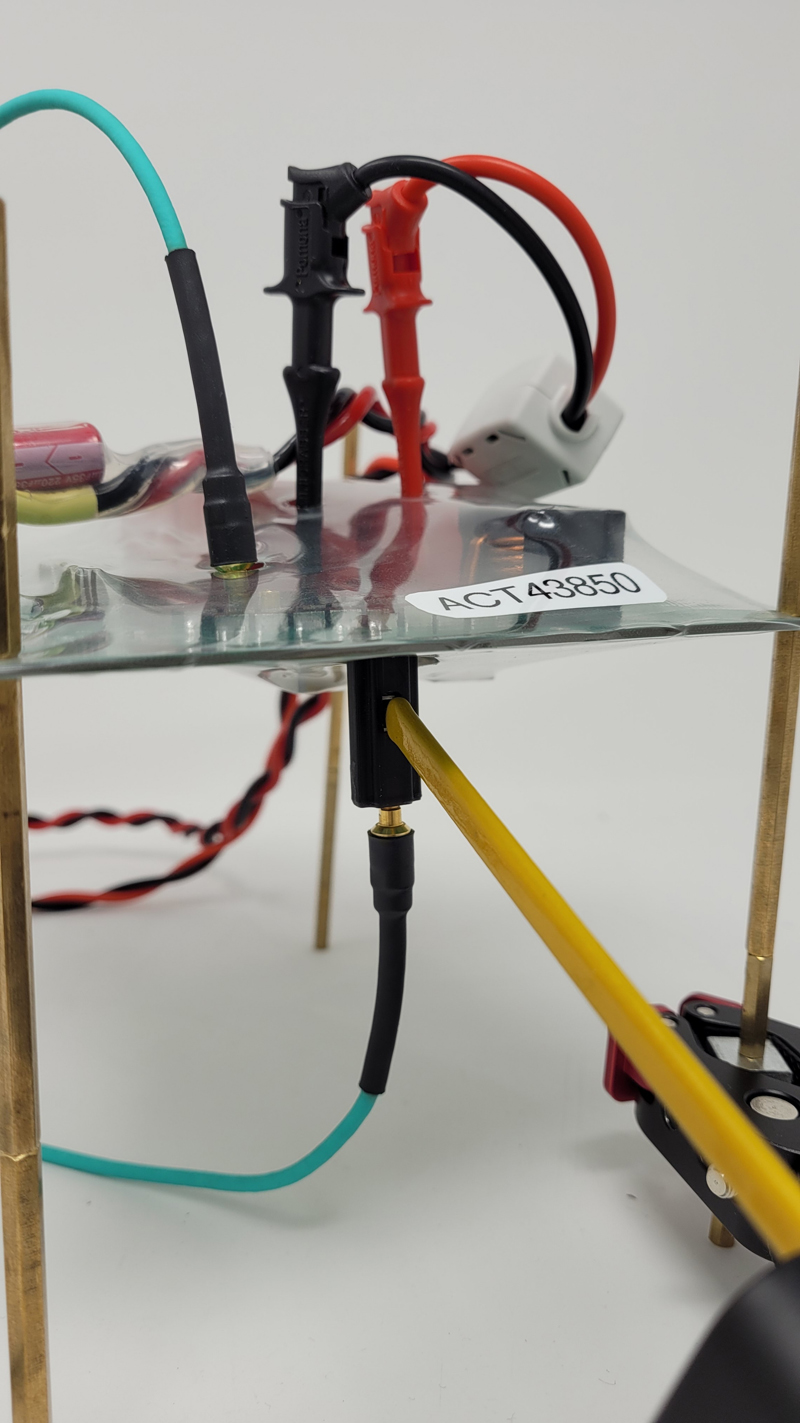
Figure 1: Test set up for VR stability evaluation
Engineers are busy replacing and updating their aged PC boards that use traditional transistors, typically super-junction silicon MOSFETs and Insulated-Gate Bipolar Transistors (IGBTs).
One hot area in this upgrading process is power supplies for pulse-load applications, such as laser pulse drivers, light beacons and RF transmitters. In this article, a voltage regulator (VR) with a 1kW pulse rating at 48V output is used as device under test (DUT) to evaluate stability, but the techniques described also apply to lower or higher voltage VRs and differing power levels.
By the nature of pulse operation, users see the benefit of reduced power loss, based on the ON-time duty cycle. This means less effort is needed in thermal/cooling design, compared with always-ON, 100% operation duty cycle power systems, where the cooling system might be a major part of the whole installation.
In contrast, pulse-load applications have their own unique challenges during the circuit design phase, and these include regulator control loop stability tests. When evaluating an always-ON system, it’s quite easy to hook up a vector-network analyzer (VNA) or a frequency response analyzer (FRA) and run a frequency sweep lasting a few minutes or so to get a Bode plot, that is, a pair of gain and phase curves to evaluate stability. As a VR for pulse loads is designed with minimal cooling, we can’t run at 100% ON duty cycle, as the prototype might dangerously overheat during the stability measurement sweep. Even if you can manage to synchronize the VNA/FRA to your pulsing load by using a gating signal input port, there is a high risk of damage to the expensive VNA/FRA, if the prototype VR crashes and an extreme surge goes to the analyzer input ports.
In this article, we examine the other well-known alternative technique to Bode plots for loop stability tests, the Step Response Test.
Small Signal vs. Large Signal
Our textbooks teach that, when you apply a transient load pulse, you can evaluate VR control loop stability by observing the output voltage excursion. However, many engineers overlook one important statement that should be written in the same page of the textbook, that statement is “…for small signals only”, and there should also be an emphasis on the problems that can occur with large signals. This condition and the difficulties it can show are common and are not limited to high power systems with WBG devices and 48V output VRs.
The key difference between ‘small signal’ and ‘large signal’ conditions is whether the regulator DC bias points move significantly during the transient or not.
As an example, testing a 5V/3A output VR with a 0A-3A load transient (you can find many plots of this condition in many VR datasheets) is a LARGE signal transient test.
When we run a large signal test, many circuit nodes both inside and outside of the VR controller chip or VR board are slewing during the 0A to 3A load step. Slew rates are practically limited and they may mask unstable behavior and, in worst cases, a VR system might oscillate, even though you don’t see any problem with this 0A-3A load step. There’s no clear boundary between what is deemed small signal or what is large signal but, in this article, we use a 0.5% perturbation in output voltage to be enough to be counted as small signal.
For further information, chapters 8 and 9 of the textbook in reference [ref1] fully explain transient (step) response, phase margin, stability and their relationship with Bode plots.
Practical testing
In the tests described in this article, we use the following equipment.
· Qorvo’s RFPoL ACT43850 prototype, as a 48V/1kW output VR. The ACT43850 utilizes a WBG transistor-based half-bridge output stage
· Oscilloscope (Tektronix MSO6) with a Power Rail Probe: TPR4000, as a VR output voltage monitor
· Picotest’s, PicoStepper (one of prototype options), as an ultra-fast 2A transient load
· PEM’s Rogowski probe, CTW Ultra-mini CWT03, as a coil current monitor
· Beehive electronics’ EMC probe 100B, as a small step current monitor
· Qorvo in-house 20A transient generator, as a dummy pulse-load
The test set up is shown in Figure 1.
Evaluation Strategy
We set up this “small signal, load transient” test as follows:
The ACT43850 RFPoL VR was powered up with its 48V output in regulation and with the output monitored with the TPR4000 voltage probe.
The load current was stepped 0A-20A-0A repetitively, to emulate the target pulsed load using the Qorvo in house transient generator, but with a sequenced, extra 2A superimposed by the ‘PicoStepper’ transient generator, resulting in an effective load on the ACT43850 of 0A-20A-22A-20A-0A
The ACT43850 output voltage response was then examined.
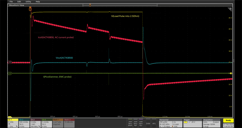
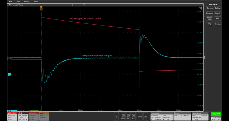
Small Signal Transient Result
Figure 2 shows the waveforms observed in the test. The initial 0A-20A step represents a ‘large signal’ transient and the subsequent 20A-22A, and 22A-20A step is a ‘small signal’ with the overall duration of the combined load cycle set at 1ms.
Click image to enlarge
Figure 2: Voltage waveforms captured in the small signal transient load response test
What we observe is the first transient step causing a large voltage excursion and settling within the 100µs. After 500µs time point, the extra 2A step causes a deviation of about +/-200mV, which settles within about 50µs. This represents about 0.5% of the 48V output so we are justified in claiming this as ‘small signal’. The 0-20A step in comparison is driving DC bias points away from their normal operating range and changing the loop response. An indication of the non-linearity produced is the different amplitude and duration of the large step voltage excursions 0A-20A and 20A-0A. Note that as a Rogowski AC current probe was used, the DC current levels in channel three show a falling value over the measurement period.
The shape of the voltage excursion with a small 2A load step indicates close to optimum damping with a phase margin of around 60 degrees, while regulating 20A, which is a good result.
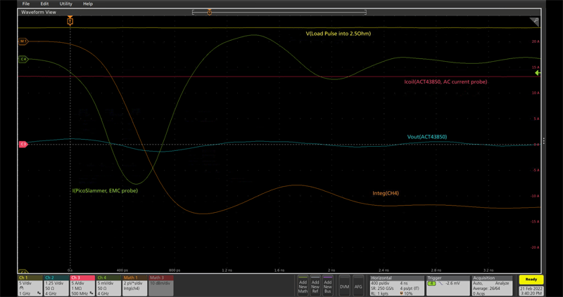
While setting up the test, the response shown in Figure 3 was seen. The anomalous overshoot of the initial 0A-20A excursion, that seems to indicate underdamping, was found to be caused by the upstream power source to the ACT 43850 going into current limit. This is an example of the spurious results that can happen with large signal pulsed load testing. As in the final test, the 2A load step shows a small excursion and optimal damping.
There are many possible effects from the large signal but figure 3 is one example.
Click image to enlarge
Figure 3: Anomalous overshoot of the VR output voltage on the initial load step was due to the upstream power source current limiting
Deeper Insights
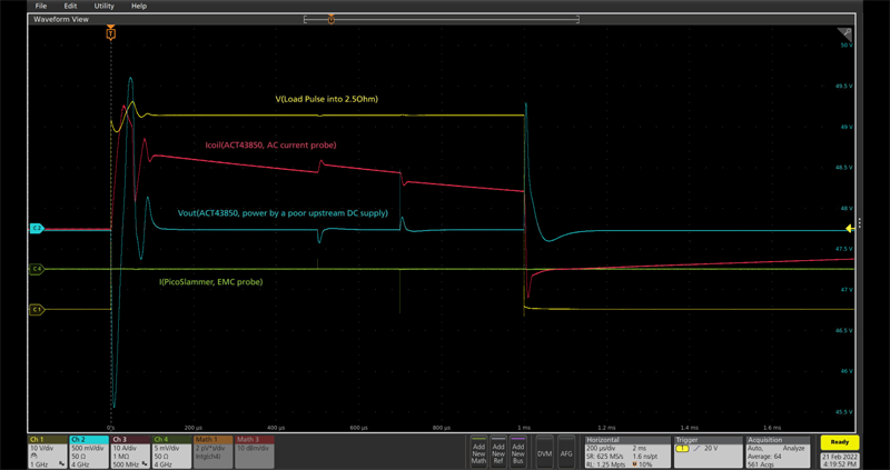
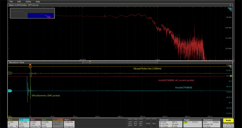
The textbooks tell us about another important condition to satisfy when we use step load (transient) response as a tool to evaluate loop stability: namely to use rise and fall edges fast enough, compared with the loop bandwidth under evaluation, and we do know that the Rogowski probe is not fast enough to capture the fast edges from the PicoStepper. However, by using the EMC probe, we can monitor the true speed of the PicoStepper, to confirm that it is fast enough. Figure 4 shows the waveforms indicated by the EMC probe.
Click image to enlarge
Figure 4: EMC probe waveforms
Channel 4 shows the 100B H-field probe’s response by zooming in closely to the falling edge of the 2A load step, showing a sub-1ns impulse. By using the integrating function of the oscilloscope, we can clearly see the shape of true current and from the Rogowski probe, we know that this absolute value is 2A falling.
By running an FFT on the channel 4 EMC probe signal, as shown in Figure 5, we can see the small signal band width. This is exactly the same waveform, but an FFT result is added. This FFT result shows that the PicoStepper transient has 700MHz bandwidth, which is enough to accurately evaluate the loop bandwidth of the ACT43850, of approximately 100kHz.
Note that in figure 2, we see a sharp spike on CH1 at 700us time point. The figure 4 is the zoom-up of that spike. Then, at CH2, we see no overshoot starting yet at this time point.
Click image to enlarge
Figure 5: FFT on the channel 4 EMC probe signal
Weak Phase Margin Example
When intentionally degrade the loop, we will see ringing as shown below.
Click image to enlarge
Figure 6: a snapshot of Bode plot reconstructed from the small signal step response in figure 2 (courtesy of Picotest)
Conclusion and Next Steps
With knowledge of the differences between small and large signal transient load testing, voltage regulators rated for pulsed loads can be evaluated successfully for loop stability.
The techniques can in theory be applied to control loop bandwidths to the 100MHz range, and for voltage regulators this is far in excess of that needed.
Pulse load stability testing can be used in applications with long connections to the end load, to identify possible ringing due to those connections, and the high measurement bandwidth possibly helps to evaluate voltage regulator stability performance in real power distribution networks.
Qorvo is working with new prototype software from Picotest to extract more detailed control loop information from these small signal response waveforms, figure 6.
References
Ref1: Fundamentals of Power Electronics: Robert Erickson: Springer