Extending the Supply Voltage of a 600 V Input, No-Optocoupler Isolated Flyback Controller to 800 V or Higher
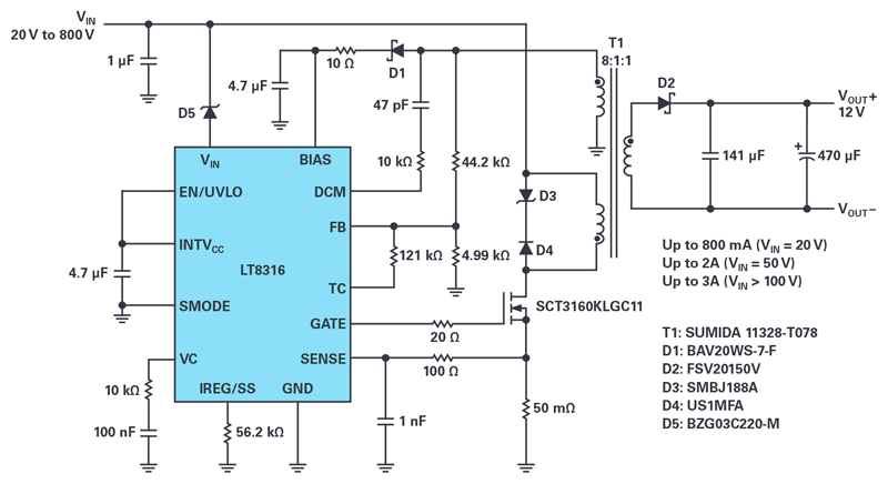
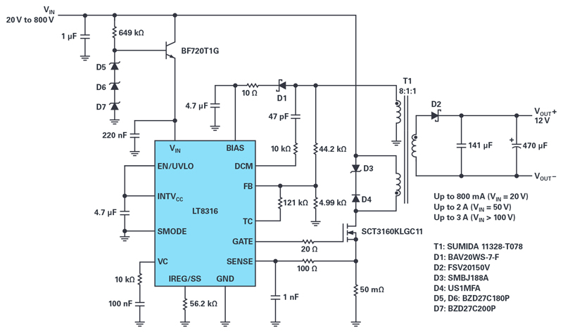
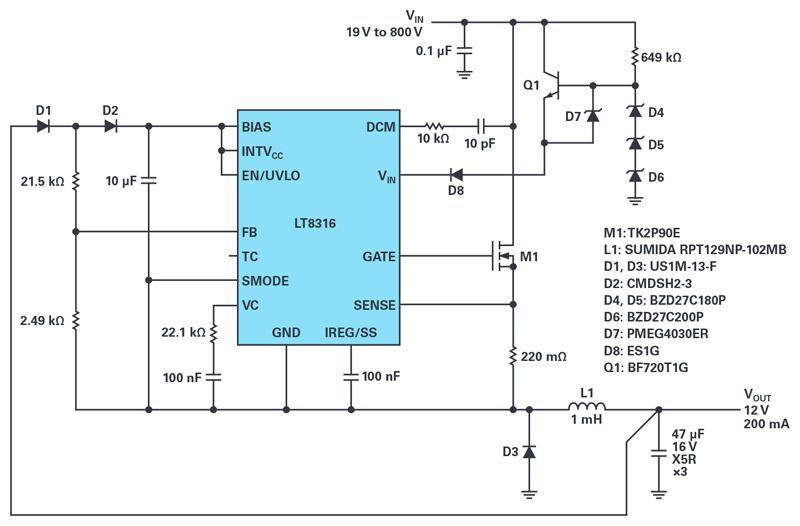
Figure 1. A complete 12 V isolated flyback converter for a wide input from 20 V to 800 V with a minimum start-up voltage of 260 V
In traditional isolated high voltage flyback converters, tight regulation is achieved using optocouplers to transfer regulation information from the secondary-side reference circuitry to the primary side. The problem is that optocouplers add significant complexity to isolated designs: there is propagation delay, aging, and gain variation, all of which complicate power supply loop compensation and can reduce reliability. Moreover, during startup, either a bleeder resistor or a high voltage start-up circuit is required to initially power up the IC. Unless an additional high voltage MOSFET is added to the start-up components, the bleeder resistor is a source of unwelcome powerloss.
The LT8316 is a micropower, high voltage flyback controller that does not require an optocoupler, complicated secondary-side reference circuitry, or additional start-up components.
Extending Supply Voltage
The LT8316 is housed in a thermally enhanced 20-lead TSSOP package with four pins removed for high voltage spacing. By sampling the isolated output voltage from the third winding, no optocoupler is required for regulation. The output voltage is programmed with two external resistors and a third optional temperature compensation resistor. Quasi resonant boundary mode operation helps to achieve excellent load regulation, small transformer size, and low switching loss, especially at high input voltage. Because the output voltage is sensed when the secondary current is almost zero, no external load compensating resistors and capacitors are needed. As a result, the LT8316 solution features a low component count, greatly simplifying the design of an isolated flyback converter (see Figure 1).
The LT8316 is rated to operate from a VIN of up to 600 V, but this can be extended by placing a Zener diode in series with the VIN pin. The voltage drop across the Zener diode reduces the voltage applied to the chip, allowing the supply voltage to exceed 600 V.
Figure 1 shows the complete schematic of a flyback converter with a wide input range of 18 V to 800 V. The guidelines for component selection are detailed in the LT8316 data sheet. With the 220 V Zener diode placed in series with the VIN pin, the minimum supply voltage for startup is 260 V, give or take, considering the voltage tolerance of the Zener diode. Note that after startup, the LT8316 will operate normally with a supply voltage below 260V.
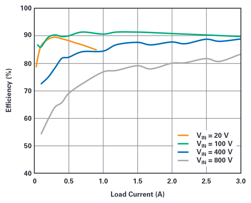
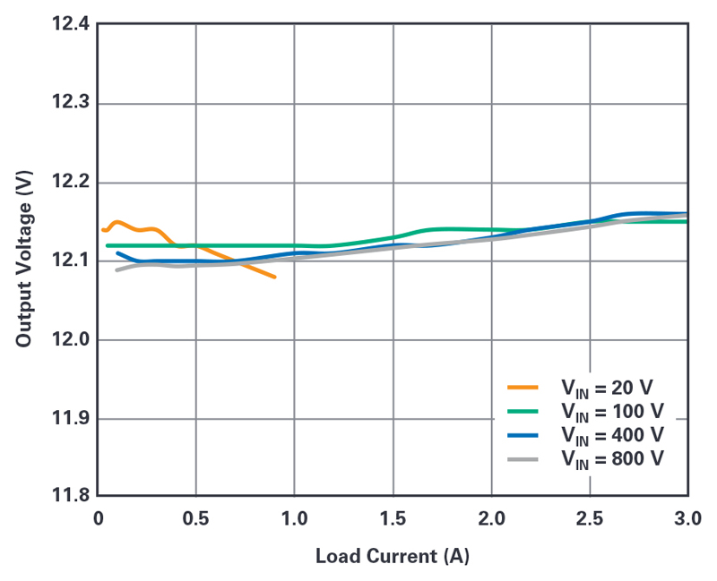
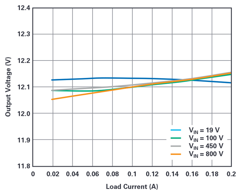
Figure 2 shows efficiency at various input voltages, with the flyback converter achieving 91% peak efficiency. Even with no optocoupler, load regulation at different input voltages remains tight, as shown in Figure 3.
Click image to enlarge
Figure 2. Efficiency of the flyback converter in Figure 1
Click image to enlarge
Figure 3. Load and line regulation of the flyback converter in Figure 1
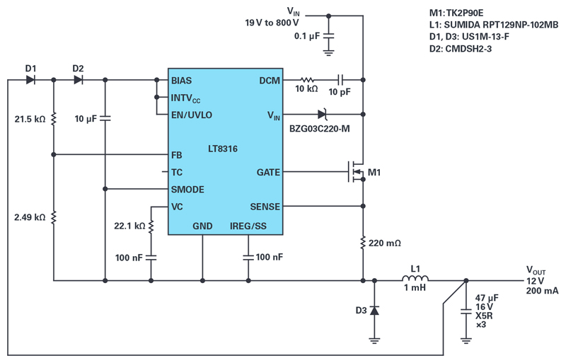
Low Start-Up Voltage Design
The previous solution extends the input voltage to 800 V, but the Zener diode raises the minimum start-up voltage to 260 V. The challenge is that some applications require both high input voltage and low start-up voltage.
An alternative 800 V maximum input voltage solution is shown in Figure 4. This circuit uses Zener diodes and a transistor to form a voltage regulator. The input voltage can safely go to 800 V with the VIN pin regulated at around 560 V. The benefit of this circuit is that it allows the LT8316 to start up at a lower supply voltage.
Click image to enlarge
Figure 4. Schematic of an isolated flyback converter: 20 V to 800 V input to 12 V, with low start-up voltage
Click image to enlarge
Figure 5. Schematic of a nonisolated buck converter with up to 800 V supply voltage
Nonisolated Buck Converter
The LT8316’s high voltage input capability is easily applied in a simple, non isolated buck converter where an isolated transformer is not required. A relatively inexpensive off-the-shelf inductor is adopted as the magnetic component.
For a non isolated buck application, the LT8316’s ground pin is connected to the switch node of the buck topology, which is a varying voltage. The unique sensing scheme of LT8316 sees the output voltage only when the switch node is connected to the ground, which leads to a simple buck schematic.
As with the flyback converter, the supply voltage of the buck converter can be extended. Figure 5 shows the schematic of a buck converter with up to 800 V input voltage. A 220 V Zener diode is placed between the supply voltage and VIN pin of LT8316. The minimum supply voltage for startup is 260 V, considering the voltage tolerance of the Zener diode. After startup, the LT8316 continues to operate normally with lower supply voltage. Figure 6 shows efficiency at various input voltages, with the buck converter achieving 91% peak efficiency. The load and line regulation is shown in Figure 7.
Click image to enlarge
Figure 6. Efficiency of the buck converter in Figure 5
Click image to enlarge
Figure 7. Load and line regulation of the buck converter in Figure 5
Click image to enlarge
Figure 8. Schematic of 800 VIN nonisolated buck converter with low start-up voltage.
Similar to the flyback converter in Figure 4, a voltage regulator can be added between the supply voltage and the VIN pin to achieve the low start-up voltage of a buck converter. It should be noted that there is a body diode from the GND pin to the VIN pin, which raises the emitter voltage of the transistor and causes base-emitter breakdown. In order to prevent this, two diodes are added to protect the transistor. The low start-up voltage solution is shown in Figure 8.
Conclusion
The LT8316 operates in quasiresonant boundary mode and requires no optocoupler for excellent regulation. In addition, it includes rich features such as low ripple Burst Mode® operation, soft start, programmable current limit, under voltage lockout, temperature compensation, and low quiescent current. The high level of integration simplifies the design of low component count, high efficiency solutions in a wide variety of applications ranging from battery-powered systems to automotive, industrial, medical, telecommunications power supplies, and isolated auxiliary/housekeeping power supplies.