Extremely Compact Isolated Auxiliary Supply for SiC-MOSFET Gate Driver
The optimal design of the isolated auxiliary supply that provides the voltage and current to drive the SiC MOSFET
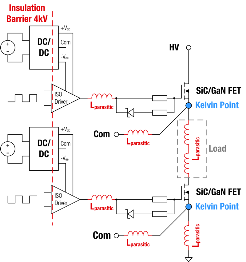
Figure 1: Topology of a SiC-MOSFET half-bridge with highlighted parasitic inductances
With the increasing spread of high-voltage power semiconductor components build with silicon carbide (SiC) technology, which operate at switching frequencies above 100 kHz, the requirements for their gate control are becoming more and more demanding. Besides the bipolar, positive and negative driving voltages for the gate driver and the EMC requirements, additional constraints regarding the protective insulation between the HV side and the Safety Extra Low Voltage (SELV) side must be considered. In addition, many applications require small size and light weight at low cost. The optimal design of the isolated auxiliary supply that provides the voltage and current to drive the SiC MOSFET is critical to help the complete gate driver system meet the many requirements set by state-of-the-art SiC applications.
1: Overview and requirements for gate control of SiC MOSFET devices
SiC MOSFETs require gate voltages of typically +15 V for full turn-on and typically -4 V for reliable turn-off. These values may vary slightly depending on the device manufacturer. Figure 1 shows a half-bridge configuration. Each SiC MOSFET requires an independent gate driver stage with its own isolated auxiliary voltage supply. This not only allows independent control of each SiC MOSFET, but also keeps the gate current loop area small, minimizing the adverse effects of parasitic loop inductance and ground disturbances caused by the very high ∆I/∆t generated during the switching transition. Otherwise, these disturbances can lead to uncontrolled turn-on and turn-off of the SiC device as well as increasing switching losses, negatively affecting the performance and reliability of the application.
2: Requirements of the Isolated Gate Driver Power Supply for SiC-MOSFETs
In high-voltage applications using SiC-MOSFET under hard-switching operation, galvanic isolation is a common requirement for safety and functional reasons. Depending on the application, basic or a reinforced isolation is required. Conventional isolated gate driver circuits "bridge" the isolation barrier, providing the required galvanic isolation.
Some of the latest high-power SiC devices or power modules can have a high total gate charge of up to 3000 nC. With an increase in switching frequency or load power, the driver system can be expected to provide 6 - 10 W of power for the most demanding current and future applications.
A critical parameter of the isolated DC-DC converter is the parasitic capacitance (Cp) between the two isolated sides. This parasitic capacitance comes from everything that bridges the barrier – the isolated gate driver and the auxiliary power transformer are key components. In the auxiliary power supply this is mainly determined by the capacitance between the primary and secondary windings of the transformer (i.e. interwinding capacitance). With latest SiC-MOSFETs switching at ∆U/∆t slew-rates of 100 kV/us, 10 pF parasitic capacitance across the barrier would cause a peak displacement current of 1 A!

Click image to enlarge
IP = displacement current
CP= parasitic coupling capacitance
With increasing Ip, distortion of the control signals as well as common mode interference currents, which affect the EMC behavior, can become considerable. The parasitic capacitance across the isolation barrier should therefore be minimized in order to reduce these adverse effects, allowing the SiC-MOSFET to switch fast, achieving with it higher efficiency, better thermal performance and a smaller solution size. It is recommended to keep Cp in the auxiliary voltage power supply below 10 pF.
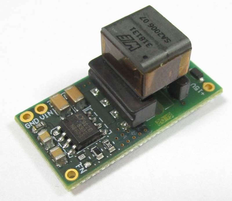
3: Würth Elektronik Solution up to 6 W
The high-performance,isolated auxiliary power supply reference design RD001 of Würth Elektronik (Figure 2) addresses these requirements and features:
· Input voltage range 9 – 18 V
· Output voltage bipolar +15 V / -4 V or Unipolar 15-20 V
· Power up to 6 W
· Peak efficiency of up to 86% (83% @ 6 W)
· Parasitic coupling capacitance less than 7 pF
· Over 50% smaller than similar DC-DC converters currently on the market: 27x14x14 mm (L x W x H)
· Weight less than 4 g
· Basic insulation for VBus 800 V
· 4000 Vrms insulation voltage pri - sec
Click image to enlarge
Figure 2: Würth Electronics reference design for a compact, isolated DC-DC converter for SiC MOSFET Gate Drivers
In addition to the PSR (primary side regulation) flyback controller from Analog Devices, the key component in the reference design is the new power transformer WE-AGDT-750318131. It uses a compact EP7 core with a customized bobbin optimized to meet the following requirements:
• Wide input voltage range: 9 to 36 V
• High saturation current of 4.5 A
• Very low interwinding capacitance of 6.8 pF typ.
• Very low leakage inductance of 270 nH typ.
for highest efficiency
• SMD pick & place ready
• Creepage & clearance distance 5 mm min.
• Safety standard IEC-62368-1, IEC-61558-2-16
• Dielectric isolation of 4 kV VAC min.
• Temperature class B 155 °C
• AEC-Q200 qualification (in progress)
The WE-AGDT series includes six transformers, all using a compact EP7 assembly and each optimized for its corresponding reference design. They provide bipolar (+15 V, -4 V) as well as unipolar (+15 to +20 V) options, with an input voltage range from 9 to 36 V and maximum output power of up to 6 W. Though optimized for SiC applications, they are also equally suitable for driving IGBT and power MOSFETs alike, and even high-voltage GaN-FETs with the correct output regulation stage.
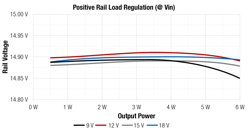
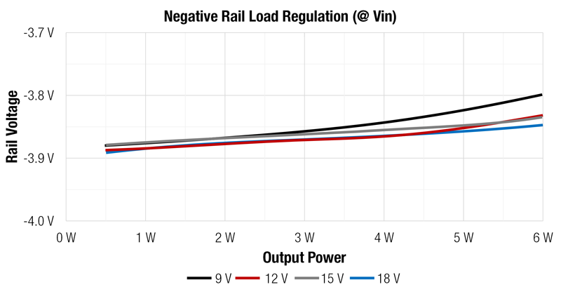
In Figure 3 the DC-DC converters output voltage regulation in dependence of the load power and the input voltage is illustrated. It can be seen that the regulation of the output voltages for an input voltage of 12 V or more is very good.
Click image to enlarge
Click image to enlarge
Figure 3a & 3b: Voltage of positive and negative rails versus load power (at Vin (nominal) = 12 V)
The simplified circuit diagram is shown in Figure 4, using the LT®8302 flyback converter in current mode, therefore the solution has a very low component count, helping to reduce overall system cost and size. The output voltage is controlled by sampling the reflected secondary voltage on the primary side, thus eliminating the need for a third transformer winding and/or an optocoupler. The controller also provides overload and output short-circuit protection for increased reliability and robustness of the auxiliary supply and delivers minimal power even at light loads to ensure accurate output voltage information and typically requires less than 0.5% of its full output power as minimum load [1].

Click image to enlarge
Figure 4: Simplified circuit diagram of the 6 WIsolated Auxiliary supply for SiC MOSFET Gate Driver
The transformer provides the galvanic isolation required between the low-voltage primary side and the high-voltage secondary side.
4: Summary
The new WE-AGDT transformer series from Würth Elektronik, together with their validated reference designs, allows electronic designers to easily implement an extremely compact and efficient auxiliary supply for SiC-MOSFET gate drivers up to 6 W. The design offers two operating voltages for the gate driver, an advanced decoupling with extremely low coupling capacitance between primary and secondary side for the high EMC requirements and a basic isolation, which withstands a DC voltage of at least 4 kV. With the bipolar and adjustable unipolar output voltage rail options provided, the designer has flexibility for selecting the optimal SiC-MOSFET drive voltages.
References:
[1]: Analog Devices, data sheet LT8302/LT8302-3 Rev. G.
[2]: Würth Elektronik, Reference design RD001, 6 W Isolated Auxiliary Power Supply for SiC-MOSFET Gate Driver
[3]: Trilogy of Magnetics; Brander, T., Gerfer, A., Rall, B., Zenkner, H., 5th ed., Waldenburg, 2018