Power supplies are being driven to operate at higher frequencies
Isolated power supply systems are prevalent in server systems, industrial applications, and telecommunication and networking equipment. In this bandwidth-hungry age of the Internet of Things (IoT), a growing number of these systems need to be efficiently powered, driving up the need for power-efficient, cost-effective solutions.
As devices get smaller, power supplies have to follow suit. Thus, designers today have one overriding objective—to maximize power per volume (W/mm3). One way to achieve this is to use higher performance power switches. There have been significant innovations in this area and exciting new products are now available that have high-speed switching capability, offering increased system efficiency and a lower component size.
These new power switches include the next generation of faster silicon-based MOSFETs as well as newer technologies like Gallium-Nitride (GaN) or Silicon-Carbide (SiC) substrates.
The new technologies’ lateral structure, compared to vertical for silicon, makes them low-charge devices and therefore capable of switching hundreds of volts in nanoseconds (ns). This is ideal for fast switching systems.
Other advantages include a higher electric field strength and electron mobility, which means the size of the switch is much smaller for a given breakdown voltage and on-resistance. Also, they have a wider band gap, which means they can operate safely at a higher current at higher frequencies.
Fast isn’t free
However, for power supplies, fast switching does not come for free—it produces high noise transients that could cause loss of modulation, or permanent damage to the overall system due to latch-up. To solve this problem, the noise immunity of components used to drive these new power switches has to be improved significantly. Let’s examine these new technologies and how designers can arm themselves to meet the power challenges of tomorrow.
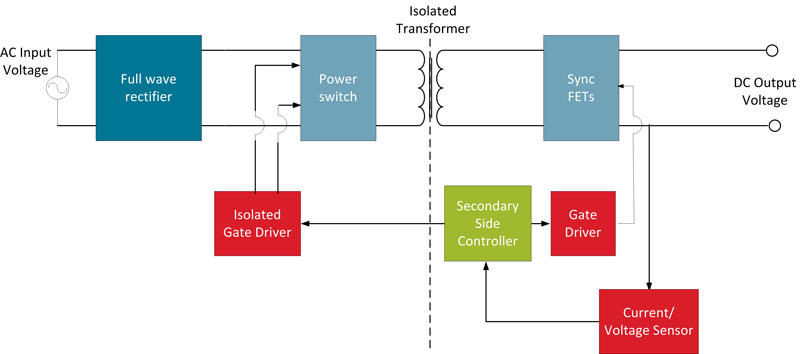
Figure 1 shows a typical ac-dc SMPS block diagram. The ac input voltage is first rectified into a dc voltage. This dc voltage is then modulated by the power switch stage using the gate drivers to control the modulation. The controller generates the control signal that the gate drivers use to modulate the power switches. This switched voltage couples through an isolated transformer with the desired turns ratio to obtain the right voltage level at the output. This voltage is then rectified by the sync FETs back to dc. The sync FETs also require gate drivers to control their switching. Current and/or voltage sensors monitor the output and provide feedback to the controller for fine tuning the modulation scheme for maximum performance.
Click image to enlarge
Figure 1. Typical ac-dc SMPS Block Diagram
Power converter system performance
As mentioned before, the challenge for designers is to achieve the highest power per volume. The best way to do this is to increase the system efficiency. The power lost through switching and/or conduction losses produces heat which has to be dissipated safely through heat sinks.
The size of the heat sink increases the total volume. Hence, creating a more power efficient design has two advantages—it increases the useful output power and reduces the total volume.
To achieve this, while maintaining safety, one of the best tools available is to increase the switching rate and frequency.
This has the following advantages:
• Faster switching time reduces switching losses and the required size of the heat sink;
• Higher modulation frequency reduces the size and cost of output capacitor and inductor;
• Higher modulation frequency reduces detrimental effect of magnetic materials (ferrites, etc.); and
• Higher modulation frequency improves transient response and prevents voltage over/under-shoot.
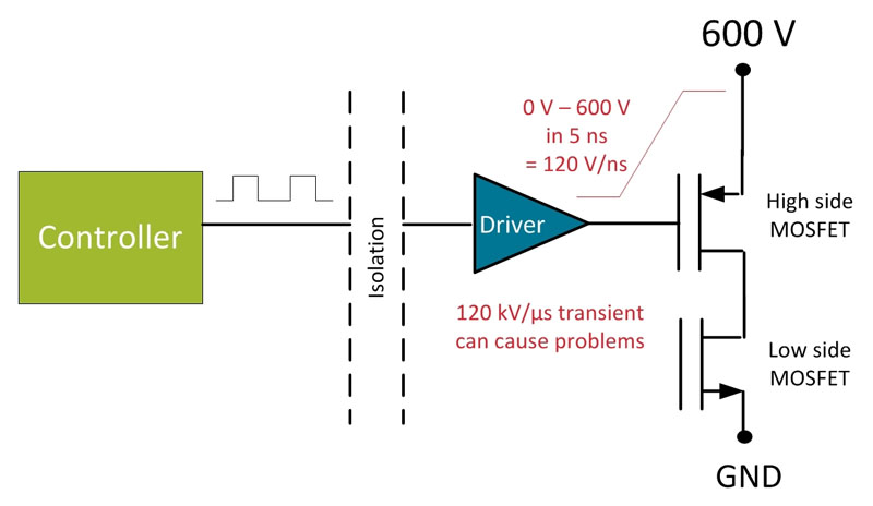
While these advantages are highly desirable, there is a risk involved. Faster switching causes higher switching transients as shown in Figure 2. Switching times in the state-of-the-art systems being designed today with GaN power switches are typically about 5ns, or about 10x - 20x faster than conventional systems. Assuming a typical 600 V high voltage rail results in a 120 kV/µs transient (600 V / 5 ns = 120 V/ns or 120 kV/µs).
Click image to enlarge
Figure 2. Switching Transients in a Power Converter
The Key Spec: Common Mode Transient Immunity (CMTI)
This high noise transient can cause the gate driver to lose signal integrity, or “glitch,” resulting in loss of modulation for the system; or worse, generate a spurious signal that could trigger both power MOSFETs to turn ON at the same time creating a hazardous electrical short condition. The high transient could also cause the gate driver to go into a permanent latch-up condition, which can also create hazardous conditions.
Gate drivers controlling the power switches have to be designed to withstand these noise transients without creating glitches or latching-up. The ability of the driver to withstand these common mode noise transients is defined by a specification that most manufacturers list in their product datasheet as common mode transient immunity (CMTI) and is expressed in units of kV/µs. For the example above, the gate driver CMTI should clearly be specified to at least 120 kV/µs.
Isolated Gate Driver Options
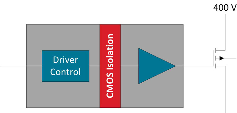
In isolated power converter systems, gate drivers need to be isolated to preserve the integrity of the isolation from the primary to the secondary side. Gate drivers typically provide up to 4A of switching current to the gate of the power FET. The larger the current driving capability, the faster the switch rates are for a given FET gate capacitance. Figure 3 shows a simple schematic of an isolated gate driver hooked up to the gate of a 400 V power FET. There are a number of isolated gate driver solutions available today.
Click image to enlarge
Figure 3. Example of Isolated Gate Driver
Junction-isolated drivers
Junction isolated drivers have a floating high side driver to accommodate the high voltage rail. The highest ratings for such devices is about 600 V. Typically, these products are economical but have a smaller tolerance to transients and can easily latch-up, causing permanent damage or a safety hazard. Typical CMTI specifications are in the range of 10 kV/µs for signal integrity and 50 kV/µs for latch-up immunity.
Opto-coupled drivers
Opto-coupled gate drivers are truly isolated (as opposed to a floating high side driver) and have been around for quite some time. Typical opto-drivers have CMTI specifications in the range of 10-20 kV/µs while the latest product offerings have much better performance, with CMTI of 50 kV/µs (MIN).
Capacitive-coupled and transformer-coupled drivers
Techniques other than junction or optical such as capacitive or transformer-coupled solutions take the performance up a substantial amount. Keeping the end goal in mind—achieving the fastest switching rates possible while maintaining safety—their biggest advantage is that they are capable of withstanding extremely high noise transients without data loss and without latch-up. Some recent transformer-coupled gate drivers specify CMTI at 50 kV/µs (MIN), which is still not sufficient for the most efficient systems we have in mind.
The latest capacitive-coupled solutions specify CMTI at 200 kV/µs (MIN) for signal integrity and 400 kV/µs (MAX) for latch-up immunity. This is industry-leading performance and best suited for the new, high frequency systems being designed today.
There are other advantages of using capacitive-coupled isolated drivers. They are fast (low latency), and the channel-to-channel and part-to-part matching is superior to the other solutions. Propagation delay (latency) can be as much as 10x better compared to some popular opto-coupled gate drivers, while part-to-part matching can be 10x better or even more. This consistency provides the designer with another key advantage—the system’s overall modulation scheme can be fine-tuned for maximum efficiency and safety without having to accommodate specification slop.
These drivers also allow lower voltage operation (2.5 V compared to 5 V), and a wider operating temperature range (-40°C to 125°C vs. -40°C to only 105°C for optos). They also offer other advanced features such as input noise filters, asynchronous shutdown capability, and multiple configurations such as half bridge or dual independent drivers in a single package.
Product safety and long term reliability is also a key concern in such applications and it is important to consider these attributes as well. Again, the new drivers are rated to 60 years of operating life at high-voltage conditions, longer than any other comparable solution.
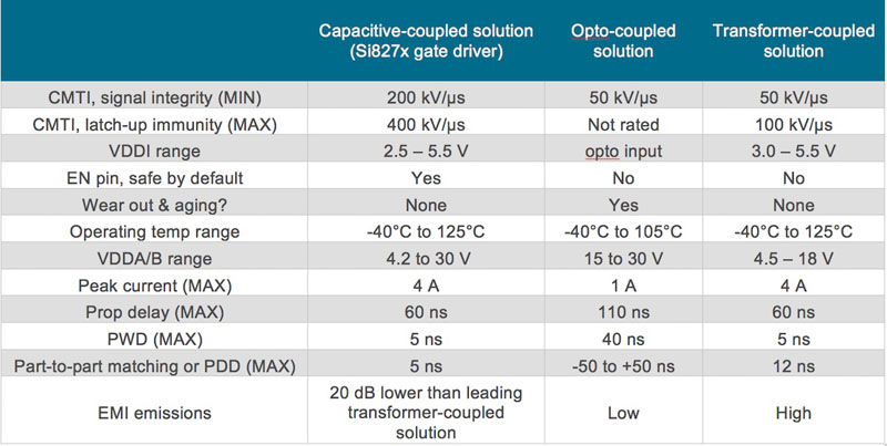
Table 1 summarizes the key comparison with competing drivers.
Click image to enlarge
Table 1. Detailed Comparison of Popular Isolated Gate Driver Technologies
Maximizing performance
Power supply designers want to maximize their W/mm3 by using the fastest power switching technology available. The latest GaN- and SiC-based switches are the fastest available technology today, but require gate drivers with very high noise immunity (CMTI).
The latest capacitive-coupled gate drivers from Silicon Labs meet GaN’s and SiC’s noise immunity requirements with margin to spare (120 kV/µs required, 200 kV/µs supplied). The new Si827x isolated gate drivers allow designers to maximize system efficiency and W/mm3 with the latest technology (see Figure 4).
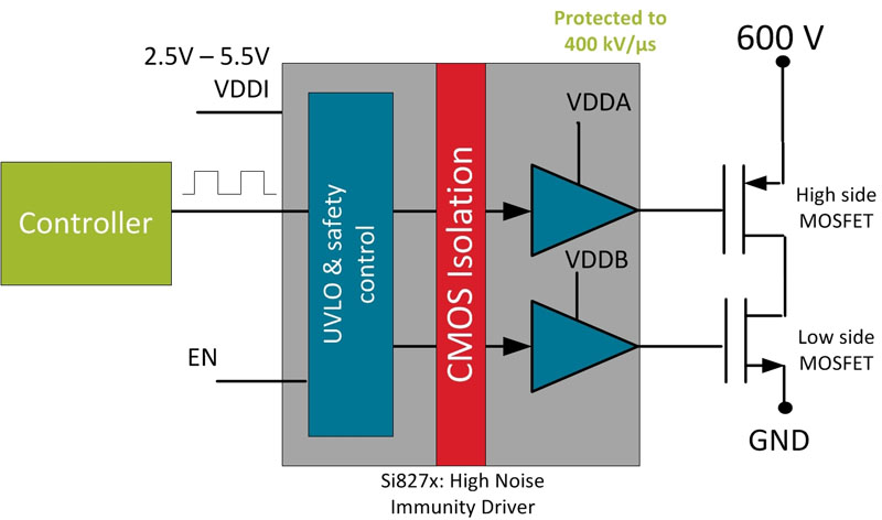
Click image to enlarge
Figure 4. Capacitive-coupled Isolated Gate Driver with High Noise Immunity