Focused Ion Beam circuit edit improves power device design
Benefits are especially significant at nanoscale geometries
Designers of power control devices and those that combine control with power FET functionality are finding that FIB circuit edit techniques proven at older process nodes are delivering even greater benefits when used at advanced technology nodes. It is also expected that FIB circuit edit techniques will be important as many power devices move to silicon carbide (SiC), gallium nitride (GaN) and other wide bandgap materials. FIB circuit edit can help designers reduce costs while optimizing performance, increasing functionality, mitigating risk and accelerating development cycles.
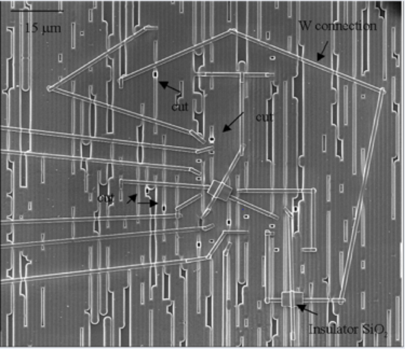
FIB systems used for circuit edit enable designers to cut traces or add metal connections inside a chip (see Figure 1). These edits can be made quickly and easily, at far lower cost than that required for a typical new wafer lot. Using the latest equipment, it is possible to edit circuits fabricated with 28 nanometer (nm) and smaller technology nodes, including devices that feature multiple-layer metal stacks and those produced in flip chip and other advanced chip scale form factors.
Click image to enlarge
Fig. 1: Front-side FIB circuit edit with multiple connections and cuts.
The FIB tool is coupled to a CAD navigation system that enables it to locate each area where edits will be made. A finely focused gallium (Ga+) ion beam with nanoscale resolution is used to image, etch and deposit materials on a device, with an extremely high level of precision. This enables designers to cut and connect circuitry within the live device, and to create probe points for electrical test. The high-energy Ga+ beam can mill through conductors, and uses various types of gases to either improve the precision of the milling process, or the ability to deposit conductive and dielectric materials.
There are numerous applications for FIB circuit edit at every commercially available node. The process can be used to verify design change on the tester, and to validate design change at the system board level.
Typical applications include:
• Debugging and optimizing devices in production
• Exploring and validating design changes
• Prototyping new devices without costly and time-consuming mask set fabrication
• Scaling fixes, so that a fix can be duplicated on a handful or tens of devices that can be provided to internal test, validation, and qualification teams and even to customers as samples
• Accelerating time to market, and/or avoiding late delivery and associated penalties
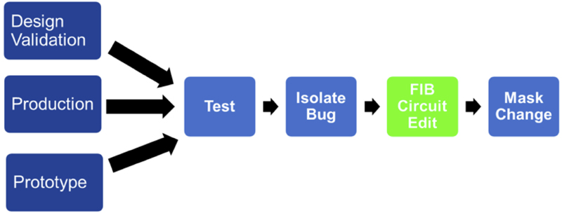
The FIB circuit edit process can be implemented both at the simulation stage and later during de-bug to optimize success rates during the IC design process (see Figure 2).
Click image to enlarge
Fig. 2: FIB circuit edit process flow.
Most current control products are fabricated using traditional silicon technology, and FIB circuit edit is performed in much the same way with these devices as it is with any other anlog or digital circuit. In the future, there is a strong possibility that drivers will move to wide bandgap materials. FIB circuit edit should offer benefits for these devices, as well. SiC, GaN and other wide bandgap semiconductor materials enable power semiconductor devices to withstand high voltages and temperatures, while providing higher frequency response, increased current density and faster switching speeds. At the same time, however, they present complex challenges related to design and characterization, process monitoring and reliability.
Challenges become even more difficult at advanced process nodes. It is harder to find and fix bugs, and mask costs are significantly higher. Testing becomes more tedious, simulations take longer, and in the case of many designs, it is impossible to achieve 100 percent verification. Additionally, there may not be perfect simulation models for extremely complex designs, and packaging can introduce stresses for sensitive devices. These challenges can be alleviated through the use of FIB circuit edit, which can be used to debug and validate fixes, and to explore design optimization changes before committing to a full mask spin.
Tips and Techniques
While some believe that FIB circuit edit only works well at 90nm and 65nm process nodes, this is inaccurate. Tool and methodology advances have enabled FIB circuit edit to be used for more precise beam guidance. Today’s systems also can operate in smaller areas, perform more intricate operations on both the back and front sides of the device, and handle copper layers.
Advances in operator skill have been particularly important. The FIB circuit edit process is not completely automated; for example, endpoint detection continues to require a high level of skill in order to ensure when selected layers of interest have been successfully etched, especially at smaller geometries and during the most challenging FIB operations.
Also important is operator knowledge about IC circuitry and process technology, ion milling patterns, and the basics of FIB tool usage. This can be difficult to achieve within an in-house operation. Larger semiconductor companies will often augment in-house circuit edit resources with external service labs. Small- and mid-sized companies generally can’t afford a $1 million FIB tool and wouldn’t likely have the staff to operate it, so they tend to go directly to external labs, which can support basic electrical design characterization or verification of redesign parameters, and have a full range of debug tools for solving difficult logic failures and other development anomalies.
Key prerequisites for FIB circuit edit success – especially at advanced nodes -- include a minimum tool resolution (or aspect ratio) of .1um, and a trenching approach that supports a finer resolution in order to make these edits. Today’s equipment can create a hole as small as 0.1x0.1um with an aspect ratio of 1/20. In the case of most 20nm and 28nm designs, it is impossible to make a small enough hole to reach the target. The solution is specialized FIB techniques that shrink the aspect ratio in order to gain access to the target. This also requires the ability to smoothly remove dummy metal above the target metal layer (which, in turn, requires deep and extensive knowledge of IC circuitry and processes, FIB tools and ion milling patterns).
Another important capability is backside and frontside editing. Despite a misperception that flipchip FIB circuit edit can only be performed from the top of a device, the reality is that backside edit is, indeed, possible -- and frequently the most effective approach. Backside edit may be required either because of the substrate material used in flipchip packaging, or because of the increased number of metal circuit layers in today’s ICs, which makes it harder to reach a lower layer when editing from the top. Figure 3 shows a typical back-side FIB circuit edit in which a probe pad is formed for micro probing.

Click image to enlarge
Fig 3: High-resolution trenching enables edits at advanced nodes. [Image courtesy of FIB International Inc.]
A third area that should be considered is the ability to handle copper layers. Most 28nm and 20nm devices are copper devices that feature a crystal structure. The engineer must have experience in using special methods that ensure metal is removed smoothly with a very high level of quality. Also, accurate beam positioning is more challenging for copper metal devices due to the non-visibility of the circuit patterns. This is also important for aluminum metal devices if there are no unique patterns to recognize on the top level.
Beyond basic FIB circuit-edit expertise it is also important that designers have access to companion failure analysis and test tools, expertise and capabilities. Most devices must ultimately be packaged, and there should be a smooth transition to de-capping or de-lidding the devices and performing micro-probing and other de-bugging tests on FIB-edited parts.
Finally, designers should consider the expertise that is required in the area of front-end processes and materials. Semiconductor advanced technology nodes create challenges related not only to nano-scale geometries, but also new front-end materials. It can be extremely valuable when the FIB circuit edit function is part of a larger lab environment with significant front-end process understanding and materials expertise.
The design verification and validation of power devices will continue to grow more difficult as the industry moves to smaller nano-scale geometries and wide-bandgap materials. FIB circuit edit is becoming increasingly important for improving design success. Thanks to advances in tools, techniques and operator skill, FIB circuit edit can be used to explore design optimization opportunities, and to debug and validate fixes, without the cost or time required for a full mask spin.