Author:
John Woodward, Executive Business Manager, Industrial Power, Maxim Integrated
Date
04/23/2018
 PDF
PDF
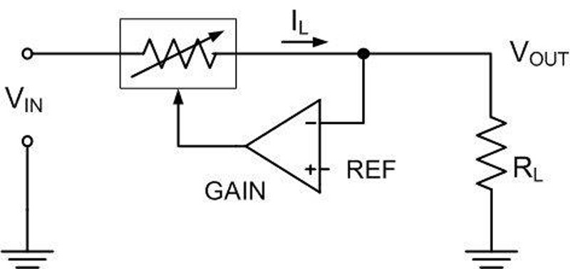
Figure 1: Linear regulator
Electronic equipment uses ICs in order to function, requiring a DC voltage as the supply input at various voltage levels. The AC power line (utility supply wall outlet) or DC power (batteries, solar panels, etc.), are the main power inputs. DC-DC power conversion technology enables these energy sources to be then converted to suitable end voltages for powering ICs and other devices.
For DC-DC step-down conversion without isolation, we have a choice of ‘linear’or ‘switching’regulator technology. A linear regulator (Figure 1) simply inserts an electronically variable resistor (a trans-resistor = transistor) in series with the input DC to drop the voltage to the desired value. If the input or load current changes, the resistor is varied by a feedback loop to keep the output voltage constant. The big disadvantage is power loss—the resistor sees the difference between input and output voltages continuously while passing the load current. At low power this is not necessarily an issue, but imagine a 5V load at 10A from a DC source of 10V. The power loss through the resistor in this case is 50W, with a conversion efficiency of only 50%.
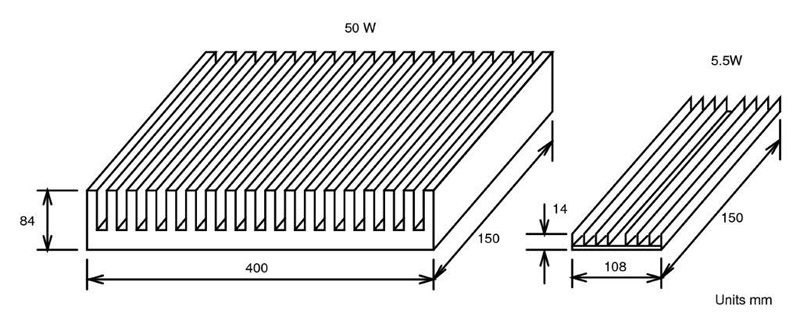
Switching regulators can provide a massive improvement in conversion efficiency and, consequently, energy savings. Transistors are employed here as well, but instead of using them in a ’linear’variable resistor mode, we use them in ’switched mode’as switches that are either in the ON or OFF state. When ON, a switch drops very little voltage across it, and when OFF, it passes very little or no current. Therefore, in either condition the power dissipated is low. Efficiencies of over 90% are achievable with this approach. If we were 90% efficient in our example above, the converter would dissipate just 5.5W compared to 50W. Figure 2 shows what a difference this would make to the size of a heatsink needed to minimize the temperature rise to only 10 degrees. The size and weight advantage is obvious. In practice, however, most modern DC-DC converters are efficient enough to eliminate heatsinks altogether and just rely on the copper planes in the PCB for dissipating the heat.
Click image to enlarge
Figure 2: Comparison of heatsinks for 50W v. 5.5W for 10⁰C rise
A Closer Look at the Basics of a Step-Down Switching Regulator
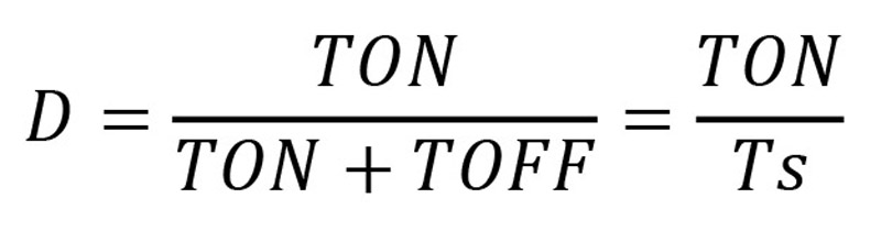
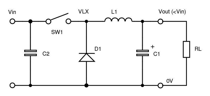
Let’s look at the basics of a switching regulator in a little more detail. Figure 3 shows a buck, or step-down, converter, which converts a given DC input voltage to a lower DC output voltage. When SW1 is ON, (Vin-Vout) is applied across the inductor, simultaneously storing energy in the magnetic field and supplying energy to Vout. When SW1 turns OFF, the current through L1 cannot instantaneously change and continues to discharge its energy to the load, RL and C1. As a result, the current in L1 falls, causing the polarity of the voltage across L1 to reverse. The switching node VLX, between D1 and L1, now ‘flies’negative until it goes below ground, forward-biasing D1 and setting up the ‘free-wheeling’path for the current in L1 to continue to flow to the output. During regulation, SW1 is toggled between ON and OFF at a fixed frequency Fsw, as shown in Figure 4. The ratio of the SW1 ON-time to the total switching cycle period Ts is called the duty cycle, of the converter ‘D’, defined as:
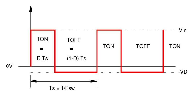
Thus, VLX is a fixed frequency, and in this case, fixed duty cycle pulse train that alternates in magnitude between Vin and -VD, that is applied to a low pass L-C filter formed by L1 and C1, where VD is the voltage drop across the diode D1. The components in the VLX pulse train are the switching frequency Fsw and a DC component whose value is equal to the average value of the pulse train over one switching period Ts. From basic mathematics and the definition for duty cycle D above, the average value of the VLX pulse train in Figure 4 may be derived to be:

If the cutoff frequency of the L-C filter is chosen to be much lower than Fsw, then Vout will be a DC voltage equal to VLXavg with a small ripple component at switching frequency Fsw. Thus,

In modern DC-DC converter circuits, D1 is replaced by a MOSFET to reduce voltage drop and improve efficiency, especially when the required output voltage is low. In this case, the voltage drop VD is negligible and may be assumed to be zero, thus resulting in the familiar step-down converter conversion equation:
Click image to enlarge
Figure 3: Step-down or buck converter
Click image to enlarge
Figure 4: Step-down or buck converter VLX node waveform
Maintaining a Constant Output
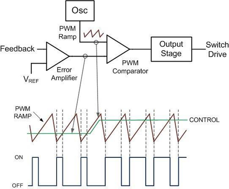
To keep the output constant over a given input voltage and load current range, we need to derive a scheme in which we monitor the output voltage and control the switch ON-times. To achieve a varying switching duty cycle of SW1, or pulse-width modulation (PWM), we first use an error amplifier to generate a DC signal which is proportional to the difference between the feedback from the output voltage and a fixed reference voltage. This signal is then compared with a sawtooth-shaped voltage at the desired switching frequency. You can see the outline in Figure 5, where the comparator and output stage in sequence give a positive voltage when the error signal is higher than the sawtooth and a low voltage when it is lower. As error voltage Vcontrol moves up and down the sawtooth, the PWM output pulse width changes in proportion from narrow to wide or 0 to 100% duty cycle. If the output voltage is low, because Vin has decreased or the load has increased, the error signal goes higher, producing a wider pulse letting more energy through SW1, increasing the output voltage back to its proper value. If the output voltage is high, the opposite happens. The output-to-input voltage ratio is simply the value of the duty cycle value, as explained in the previous section.
Click image to enlarge
Figure 5: PWM scheme
Stepping-Up Voltages: the Boost Converter
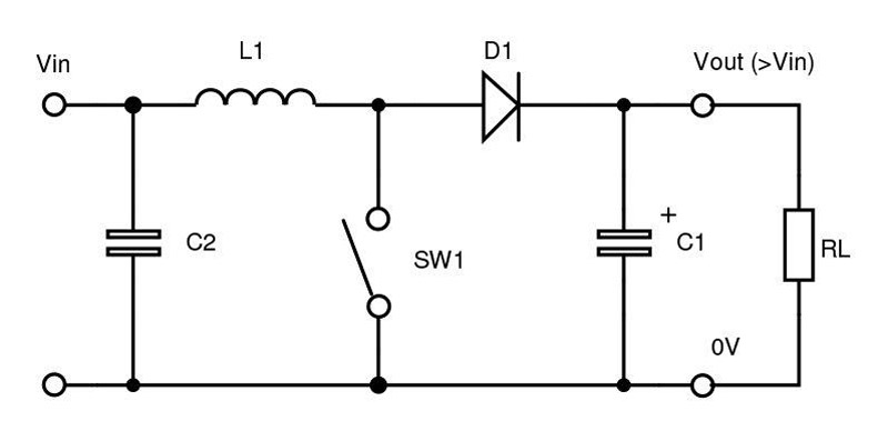
If you need the output voltage to be higher than the input, the same components can be rearranged into the boost configuration, shown in Figure 6. In the buck converter, current flows directly from input to output for the switch ON-period with the inductor-stored energy filling in when the switch is off. In the boost converter, the energy flow is quite different. The total energy required for each cycle is stored in the inductor during the ON-time of SW1 and then released during its OFF-time. As before, inductor current cannot abruptly stop, so when SW1 turns off and the inductor current tends to fall, the switching node of D1 and SW1 flies positive to force this current, forward-biasing D1 and passing energy to the output. The positive voltage can theoretically be any value higher than the input, and duty cycle control similar to the buck converter is used to keep the voltage in regulation. The equation for the conversion ratio of the boost converter may be derived using similar principles outlined for the buck converter to be:
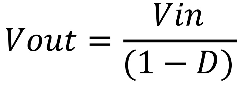
Click image to enlarge
Figure 6: The boost or step-up converter
Inverting and Stepping Up or Down the Voltage: the Inverting Buck-Boost Converter
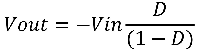
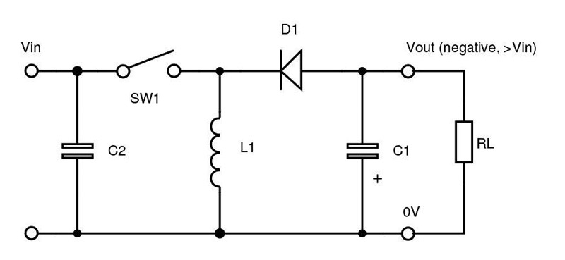
Another re-arrangement of the same components with respect to the input and output voltage terminals is possible, and results in the buck-boost converter shown in Figure 7. Here, the output voltage polarity is inverted or ‘negative’with respect to the input and the magnitude of Vout can be varied with duty cycle control to be anywhere from zero to any high negative value. In this case the conversion ratio of the boost converter may be derived using similar principles outlined for the buck converter to be:
Click image to enlarge
Figure 7: The inverting buck-boost converter
State-of-the-Art Converters Integrate Multiple Capabilities
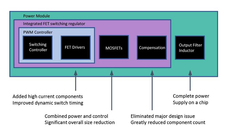
High efficiencies are regularly achieved in all these topologies and even the historical problem of switching noise has receded with better control and better power switching schemes. For all three converters, the control electronics of error amplifier, oscillator, sawtooth generator, and comparator have all been integrated into a single chip. Many of these types of feature-set flavors are available from suppliers such as Maxim. Features are varied and comprise of over-load sensing, over-temperature shutdown, input under-voltage sensing, and much more. Maxim’s power conversion technology evolution is shown in Figure 8.
Click image to enlarge
Figure 8: Evolution of high-density power conversion integration at Maxim
A second level of integration came with the inclusion of the driver stage onto the chip, and then a major leap forward came when the power MOSFETs themselves were included. Next came the inclusion of programming and loop compensation components, which really helps the overall component count and relieves the designer of the often-iterative task of loop stabilization.
The toughest challenge for semiconductor technology in general has been to integrate the L-C filter. Here, basic physics gets in the way. The inductor and capacitor are both energy storage elements that have physical volume. However, with the improved efficiency of MOSFET technology, Maxim has been able to successfully increase switching frequencies and reduce the capacitor and inductor values and physical sizes to a point where advanced packaging technology can be used to co-package these elements into one highly efficient, easy-to-use power module that enables a ’power supply in a box’plug-and-play solution for system developers.
You can learn more about power switching technology in a video from Maxim hosted by Bob Mammano, the father of the first switch-mode power supply, https://www.youtube.com/watch?v=Q0E-ZAsqzKE. This is the first in a series of power system design videos which take viewers from the basics all the way through the more complex topics from the fascinating world of power-switching technology.
Maxim Integrated