GaN-Based Design of a 2 kW 48 V/12 V Bi-Directional Power Module for 48 V Mild Hybrid Electric Vehicles
With the increase in government mandates to combat climate change, automakers are moving quickly to leverage new technology to respond by switching from the internal combustion engine to electric-drive vehicles
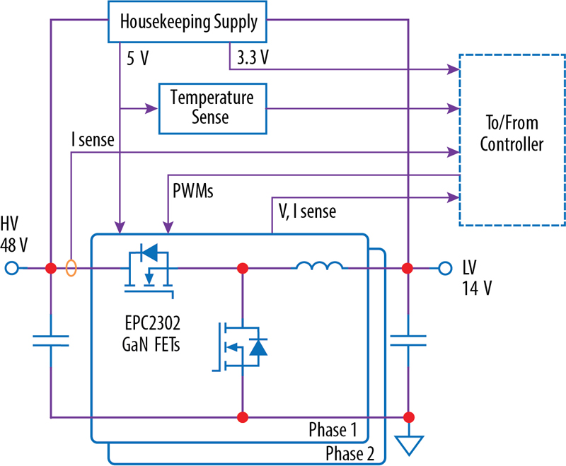
Figure 1: Simplified schematic diagram of the bi-directional converter
The hybrid vehicle market has more than doubled from 2017 from 2.0% to 5.1% and by 2025, one of every 10 vehicles sold worldwide is projected to be a 48 V mild hybrid. 48 V systems boost fuel efficiency, deliver four times the power without increasing engine size, and reduce carbon-dioxide emissions without increasing system costs. These systems will require a 48V – 12V bidirectional converter, with power ranging from 1.5 kW to 6 kW. The design priorities for these systems are size, cost, and high reliability. GaN-based designs provide a solution to address all these priorities.
This article presents the design of a 2 kW, two-phase 48 V/12 V bi-directional converter using GaN FETs that achieves 96% efficiency and is targeted for the 48 V mild hybrid system. A scalable solution: two converters can be paralleled for 4 kW, three converters for 6 kW or only one phase can be used for 1 kW. A simplified schematic of the bi-directional DC-DC converter is shown in Fig. 1.
Design of the 48 V/12 V Bi-directional DC-DC converter
This design uses the EPC2302 GaN FET which has a low inductance 3 x 5 mm QFN package with exposed top for excellent thermal management. With 1.8 mΩ RON, the rated peak dc current is 101 A. Therefore, a two-phase approach is selected so that the FET current requirement is reduced. As an example, at 14 V 2 kW output, the dc current in each phase is 70 A. This also reduces the current rating requirement for the inductors.
The MPQ1918-AEC1 gate drivers in this design are AEC-Q100 qualified and use bootstrap technique with voltage clamping for driving the high side FET. These drivers also have fast propagation times and excellent propagation delay matching of less than 1.5 ns typical.
Vishay IHTH-1125KZ-5A series inductors offer high current ratings for the inductance. In this design, the 1.0 µH inductor and 500 kHz switching frequency is selected, resulting in 80 A peak inductor current.
To ensure accurate phase current balancing, current sensing using precision shunt resistor is preferred over inductor DCR current sensing. The MCP6C02 current sense amplifier used in this design, has a maximum bandwidth of 500 kHz and 50 V/V gain. This results in 10 mV/A total current sensing gain for 0.2 mΩ shunt.
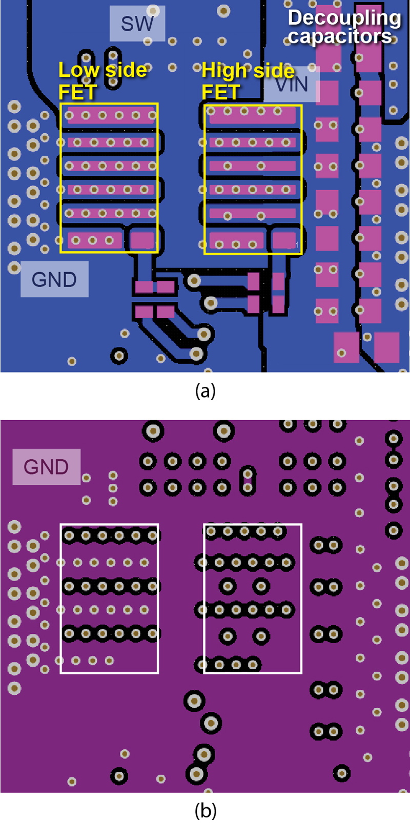
Symmetrical layout between the two phases is also critical in phase current balancing and minimizing other effects from mismatch, such as gate drive delay, switching transition speed, overshoot, etc. Figure 2 shows the layout example around the GaN FETs in this design, which utilizes an internal vertical layout technique by placing the decoupling capacitors close the FETs with a solid ground plane underneath.
Click image to enlarge
Figure 2: Example layout of the top two layers of the printed circuit board around GaN FETs: (a) top layer consisting of ground (GND), switching node (SW) and input (VIN) nets, and (b) middle layer 1 of solid ground plane
Digital Control
A dsPIC33CK256MP503 digital controller from Microchip is used in this design. It is a 16-bit processor with a maximum CPU speed of 100 MIPS. The pulse- width modulation (PWM) module can be configured in high-resolution mode, resulting in 250 ps resolution in duty cycle and dead times, allowing accurate adjustment of dead times to fully exploit the fast-switching capability of the GaN FETs.
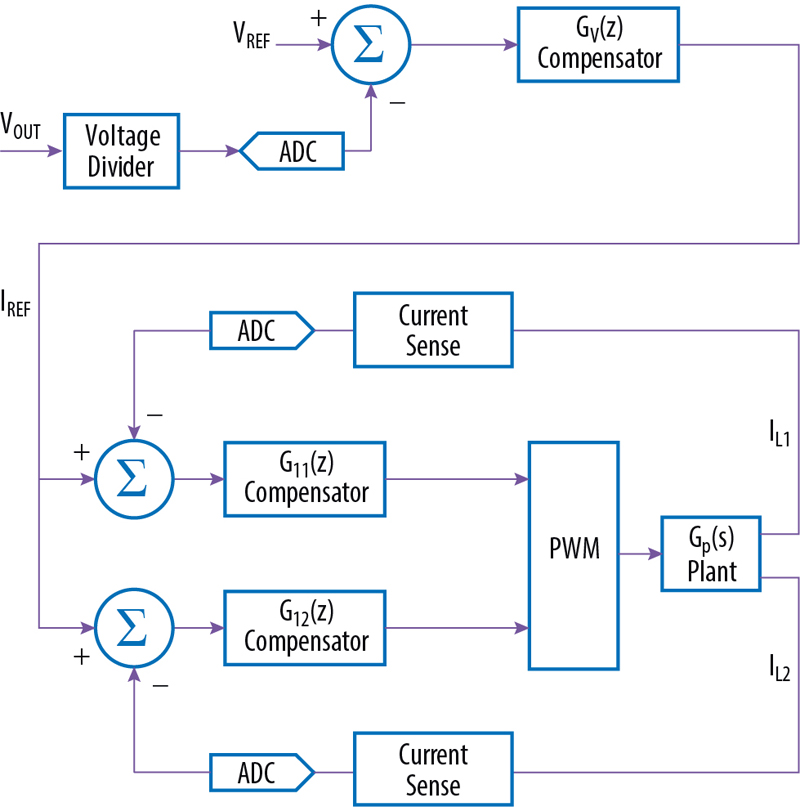
Digital average current mode control is implemented for both buck and boost modes. The current sensing circuitry consists of sense resistors and differential amplifiers. In this design, low loss 0.2 mΩ sense resistors and low-noise amplifiers MCP6C02 are used. The control block diagram is shown in Fig. 3. The same current reference IREF is used for the two independent current loops. As a result, the current in both inductors will be regulated to the same value. The bandwidth of the two inner current loops are set to 6 kHz, and the outer voltage loop bandwidth is set to 800 Hz.
Click image to enlarge
Figure 3: Digital average current mode control diagram
Thermal Management
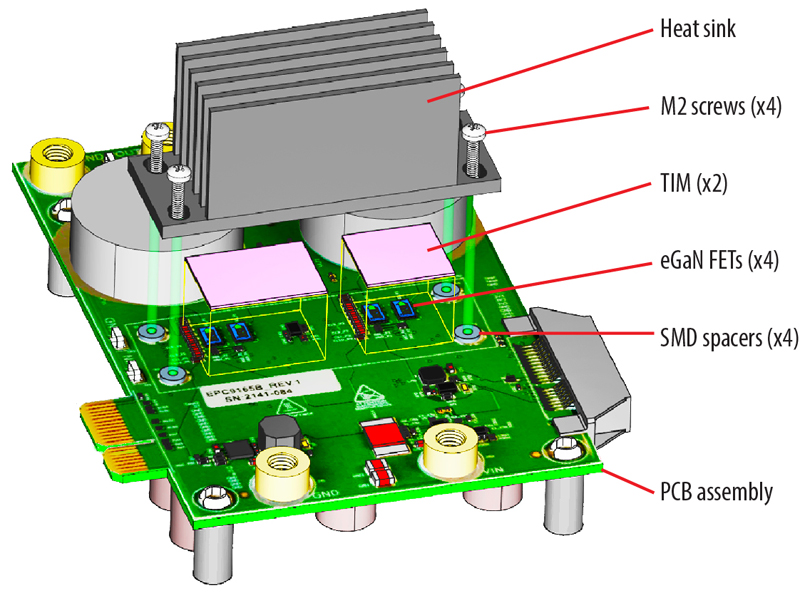
For the end-use case of vehicle electrification, the heatsinking capability can be considered infinite since this will ultimately function inside a vehicle with the unit mounted to the chassis. For this design, at full output power of 2 kW, a standard commercially available 8th brick heatsink is used here. Four metal spacers are installed on the PCB to provide the appropriate clearance for the heatsink mounting. A thermal interface material (TIM) is required between the FETs and heatsink. Usually, the material needs to have a) mechanical compliance due to compression, b) electrical insulation and c) good thermal conductivity. In this design, a TIM with 17.8 W/mK is used. Figure 4 shows the 3D heatsink installation view.
Click image to enlarge
Figure 4: Heatsink installation view, showing the metal spacer, thermal interface material
Design Validation Results
Figure 5 shows a photo of the EPC9165 [6] converter without the heatsink mounted. The dimensions are 4.3x2.8x1.6 inches (108x70x40 mm) excluding the edge connectors.

Click image to enlarge
Figure 5: Photo of the EPC9165 converter with the EPC9528 dsPIC33CK controller module attached
With the heatsink installed and 1700 LFM airflow, the converter was operated at 48 V input, 14.3 V output and tested at 500 kHz. The efficiency results in Fig. 6 show that at 500 kHz, using a 1 µH inductor, the converter achieved a peak efficiency of 97%. The converter was also tested at 14.3 V input and 48 V output for boost mode operation, as shown in Fig. 7.
At full load, EPC eGaN FETs can operate with 96% efficiency at 500 kHz switching frequency, enabling 1 kW/phase compared to silicon-based solutions, which are limited to 600 W/phase due to the limitation on the inductor current at 100 kHz maximum switching frequency.

Click image to enlarge
Figure 6: Measured converter efficiency at 500 kHz, 48 V input and 14.3 V output

Click image to enlarge
Figure 7: Measured converter efficiency at 500 kHz, 14.3 V input and 48 V output
Conclusions
With increasing global legislation aimed at higher fuel efficiency standards, vehicle manufacturers are searching for cost-effective solutions to meet these demands while still providing the power required for ever-increasing electronically driven functions. The design of GaN-Based bi-directional high-power converter for mild-hybrid cars and battery power backup units can meet the design priorities for system size, cost, and high reliability. This scalable solution can be used to meet the power requirements of the latest 48 V mild hybrid systems, with power ranging from 1.5 kW to 6 kW.


