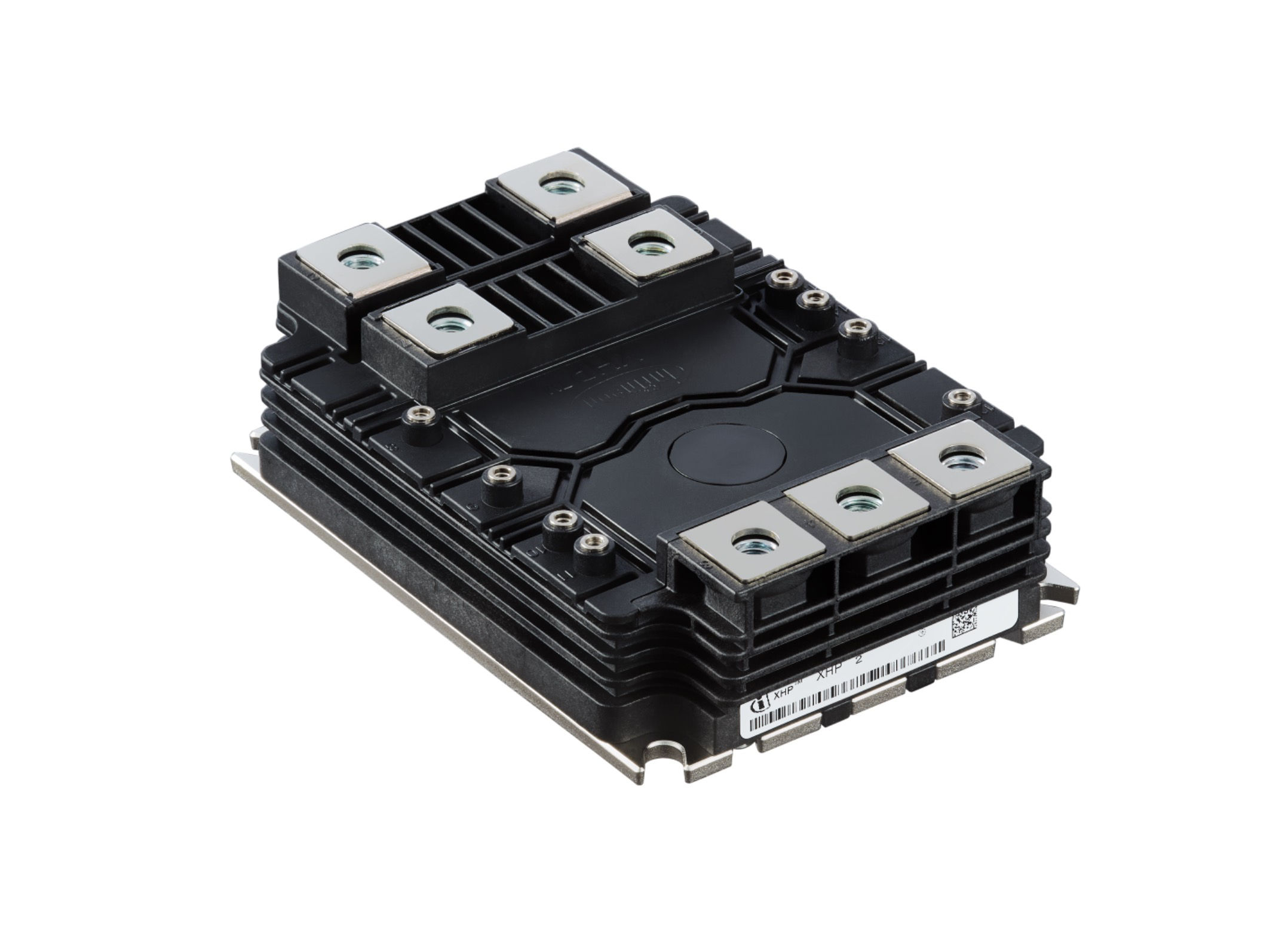
GaN FET with Integrated Driver and Active Power Management

Engineers can deliver twice the power density and the highest efficiency in their automotive onboard chargers and industrial power supplies
Texas Instruments (TI) expanded its high-voltage power management portfolio with the next generation of 650-V and 600-V gallium nitride (GaN) field-effect transistors (FETs) for automotive and industrial applications. With a fast-switching, 2.2-MHz integrated gate driver, the new families of GaN FETs help engineers deliver twice the power density, achieve 99% efficiency and reduce the size of power magnetics by 59% compared to existing solutions. TI developed these new FETs using its proprietary GaN materials and processing capabilities on a GaN-on-silicon (Si) substrate, providing a cost and supply-chain advantage over comparable substrate materials such as silicon carbide (SiC).
Vehicle electrification is transforming the automotive industry, and consumers are increasingly demanding vehicles that can charge faster and drive farther. As a result, engineers are being challenged to design compact, lightweight automotive systems without compromising vehicle performance. Using TI’s new automotive GaN FETs can help reduce the size of electric vehicle (EV) onboard chargers and DC/DC converters by as much as 50% compared to existing Si or SiC solutions – enabling engineers to achieve extended battery range, increased system reliability and lower design cost. In industrial designs, the new devices enable high efficiency and power density in AC/DC power-delivery applications where low losses and reduced board space are important – such as hyperscale and enterprise computing platforms as well as 5G telecom rectifiers.
Double power density with fewer devices
In high-voltage, high-density applications, minimizing board space is an important design consideration. As electronic systems are getting smaller, the components inside them must also get smaller and sit closer together. TI’s new GaN FETs integrate a fast-switching driver, plus internal protection and temperature sensing, enabling engineers to achieve high performance while reducing board space for their power management designs. This integration, plus the high power density of TI’s GaN technology, enables engineers to eliminate more than 10 components typically required for discrete solutions. Additionally, each of the new 30-mΩ FETs can support up to 4 kW of power conversion when applied in a half-bridge configuration.
Reach the industry’s highest efficiency in power factor correction (PFC)
GaN offers the advantage of fast switching, which enables smaller, lighter and more efficient power systems. Historically, the trade-off with gaining fast switching capability is higher power losses. To avoid this trade-off, the new GaN FETs feature TI’s ideal diode mode to reduce power losses. For example, in PFCs, ideal diode mode reduces third-quadrant losses by up to 66% compared to discrete GaN and SiC metal oxide silicon FETs (MOSFETs). Ideal diode mode also eliminates the need for adaptive dead-time control, reducing firmware complexity and development time.
Maximize thermal performance
Offering 23% lower thermal impedance than the nearest competitive packaging, the TI GaN FET packaging allows engineers to use smaller heat sinks while simplifying thermal designs. The new devices provide maximum thermal design flexibility, no matter the application, with the ability to choose from either a bottom- or top-side-cooled package. In addition, the FETs’ integrated digital temperature reporting enables active power management, allowing engineers to optimize system thermal performance under varying loads and operating conditions.
For more information, visit TI's site.