GaN Reliability: Beyond Performance and Efficiency
Delivering Optimized Reliability Through Integration
Figure 1: Integrated GaNFast Power IC
Designers are seeking alternatives to silicon to meet the performance and efficiency challenges of their next generation technologies. In addition, OEMs are looking for ways to reduce their carbon footprint by reducing materials and energy use related to their products. Gallium nitride (GaN) is rapidly becoming the semiconductor of choice as its physical properties and inherent voltage handling capabilities enable companies to address both these challenges. What’s more, in addition to performance and efficiency improvements, GaN can also make a significant contribution to enhancing system reliability.
Design Choices for Reliability
The first thing to note is that, as a wide bandgap (WBG) material GaN is fundamentally more reliable than silicon.
Bandgap is the energy needed to free an electron from its orbit around the nucleus and, at 3.4 eV, the bandgap of gallium nitride is over three times that of silicon. As bandgap determines the electric field that a material can withstand, GaN’s wider bandgap allows it to accommodate higher breakdown voltages than silicon. Not only is GaN ten times more capable than silicon of supporting higher voltages, but it also offers better thermal stability at higher temperatures. While GaN has a slightly lower thermal conductivity than silicon, this is more than offset by the significant increases in efficiency - increases that mean that at similar voltages, GaN runs cooler than silicon, reducing thermal loads and reliability issues associated with heat.
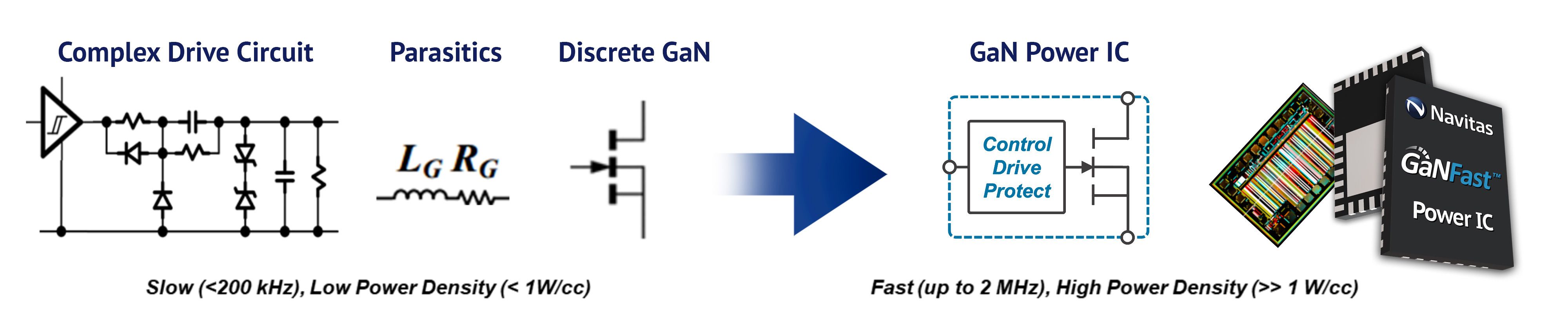
In terms of GaN IC design there are a number of factors that will contribute to the reliability of a given technology. The first is whether the GaN IC operates in enhancement mode or depletion mode.
Conventional GaN HEMT (high electron mobility transistor) technology, for example, typically deploys ‘normally-on’ depletion mode (dMode). This requires a negative gate voltage (VGS) to turn off, which is not a practical solution for offline applications as it would mean an immediate short-circuit across the AC mains. To mitigate this unwanted characteristic a second low-voltage ‘cascode‘ silicon FET is used to turn the GaN power device on and off. This not only compromises performance (the performance of the silicon FET is inferior to that of the GaN switch) but impacts reliability as a result of high parasitic inductance, a tendency for oscillation and internal overvoltage stress due to AC and DC mismatch of the GaN and silicon devices - and the need to add passive components to mitigate these effects.
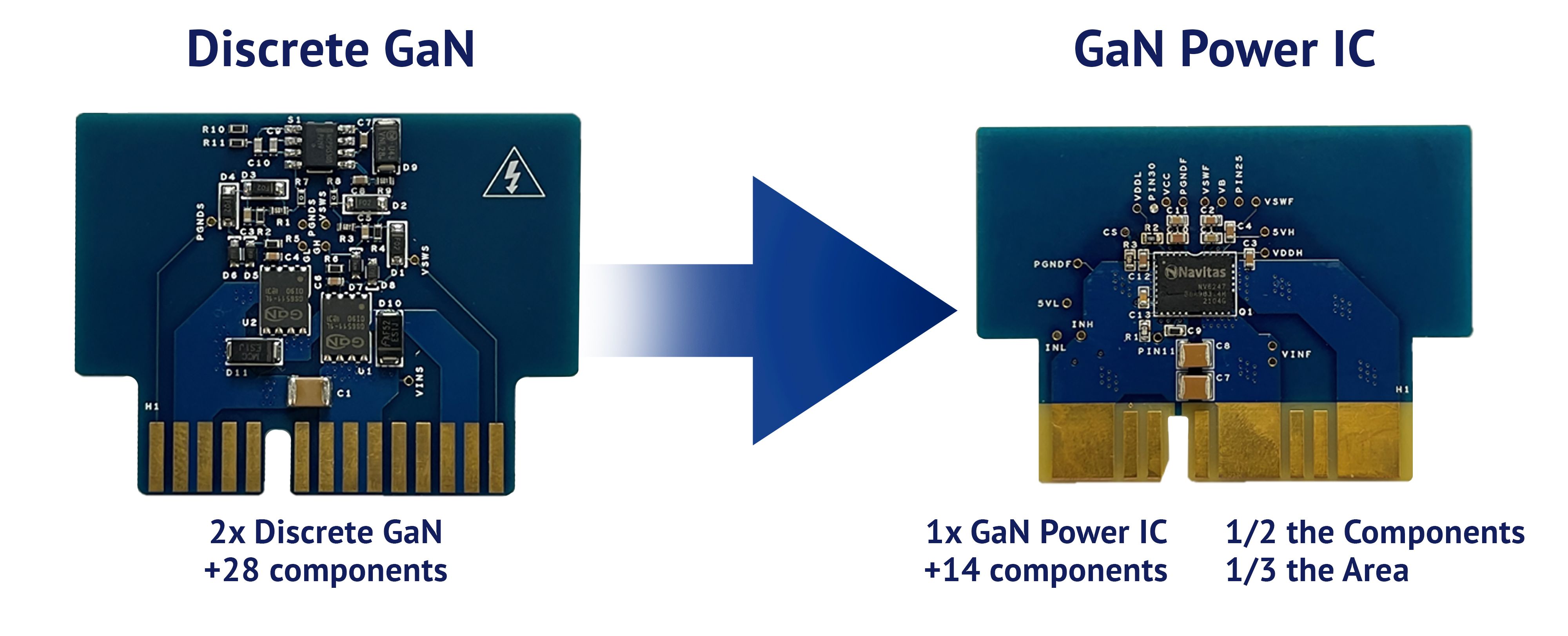
Figure 2: Fewer components translates to fewer potential points of failure
Enhancement mode (eMode) devices, on the other hand, are naturally ‘normally off’ and behave in a safe, familiar way for power design engineers in that a current flows when a positive voltage is applied to the gate. However, if the voltage is too low the GaN FET is not fully turned on, resulting in higher resistance and higher losses, which impacts reliability through increased heat. If too high, the gate structure can be damaged due to avalanche breakdown and subsequent overheating at localized spots at the gate metal pGaN schottky junction. That’s why with ‘discrete 3-terminal’ (gate, drain, source) GaN FETs, complicated structures are typically required to control the GaN gate voltage safely. Again, these add complexity and multiple points of potential failure, not to mention slowing down the switching frequency of the application and, therefore, diluting the GaN performance benefits.
Monolithic Integration
In developing its own family of products Navitas has taken an advanced approach to deliver products that both simplify circuit design and improve reliability. Using lateral 650 V eMode GaN, the company has a proprietary AllGaN process design kit (PDK) that allows the monolithic integration of GaN FET, GaN analog (drive) and GaN logic into a single GaN Power IC as shown in figure 1.
In addition to specifying the IC design elements, the Navitas GaN Power IC PDK also includes a proprietary GaN power FET design. This design, coupled with Navitas’ unique GaN power IC production test methods and extensive reliability characterization and qualification processes delivers a robust voltage withstand capability that enables power ICs with an 800 V transient rating and continuous ratings of up to 700 V.
As well as outperforming both legacy silicon semiconductors and discrete GaN devices, these ICs offer much better system reliability than either of these technologies thanks to:
● Reduced electrical stress: Fewer spikes and less overshoot and ringing translates to longer life components
● Fewer components and interconnects: Fewer components, as illustrated in Figure 2, reduces the number of potential failure points
● Increased manufacturing automation: Elimination of through-hole devices, heatsinks and wire-wound magnetics all eliminate manual labor and risk of defects or excessive manufacturing variation
The benefits of this integration can be illustrated by considering the respective waveforms of GaN discretes vs GaN power ICs as shown in Figure 3.
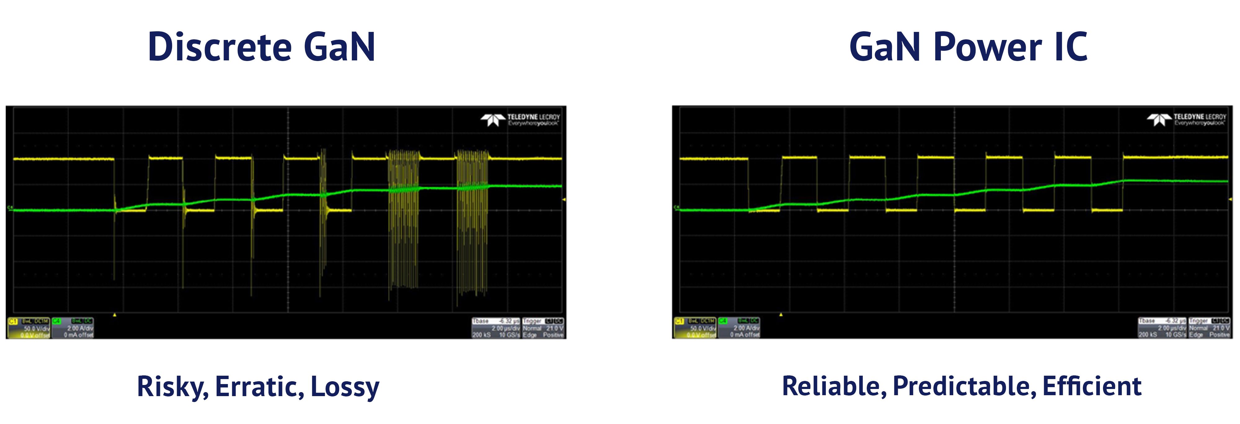
Figure 3: Waveforms of GaN discretes and integrated GaN ICs
Recently, Navitas has further increased the level of integration of its GaNFast ICs with the launch of a third generation of devices that integrate real-time, accurate and fast sensing of system parameters including current and temperature and enable a patent-pending loss-less current-sensing capability. GaNSense™ continues the evolution from legacy silicon to fully integrated GaN (Figure 4), can improve energy savings by a further 10% compared to prior generations. minimizes external component count and shrinks system footprints. And with GaNSense, if the GaN IC identifies a potentially dangerous system condition it is designed to transition rapidly to a cycle-by-cycle sleep-state, for example, with a dangerous system short-circuit condition, the GaNSense chip can go from detect to protect in only 30 ns. This enhances system reliability by protecting both the device and the surrounding system, and has been adopted by Lenovo, Xiaomi, vivo and others. Finally, thanks to the industry’s tightest current-measurement accuracy and response time, GaNSense technology reduces dangerous over-current spikes and time in the ‘danger zone’ by 50% compared to previous best-in-class solutions.
Fabrication and Packaging
The approach to semiconductor fabrication and packaging also plays an important role in device quality and reliability. Navitas GaN power ICs are fabricated by TSMC, starting with a standard silicon wafer as an inert mechanical substrate. A very thin layer of GaN is then epitaxially grown onto the top surface. From there, standard CMOS processing techniques are followed including masking, etching, diffusion and sputtering to create a completed wafer containing thousands of GaN chips. While data-processing silicon chips require complex, extremely-expensive, sub-10 nm processing equipment, GaN-on-Si production uses cost-effective, proven and widely-available 350 nm equipment ensuring maximum yields and repeatable quality and reliability.
Once fabricated, the wafers are accurately sawn into individual dice (chips) and packaged into frequency-optimized QFN packages. Navitas has been able to adapt industry-standard packaging processes to make patented high-voltage and high-power packages for GaN that are optimized for reliability.
Beyond Technology – Other Choices for Quality and Reliability
Beyond the technology there are other choices that device manufacturers can make to deliver optimum quality and reliability in real-world environments. One such choice is to develop technologies that focus on the application-specific needs of a given market rather creating a ‘one-size-fits-all’ solution. This approach gives customers in those markets the confidence that replacing legacy silicon with GaN will not compromise – and can actually improve – reliability.
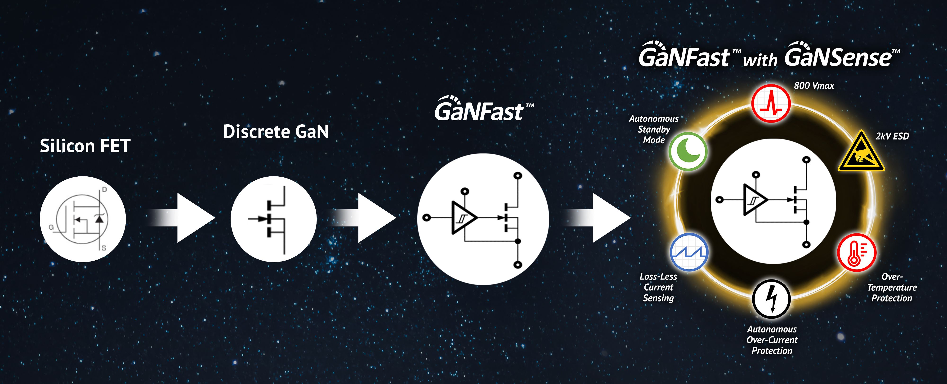
Figure 4: GaNFast power ICs with GaNSense technology further enhance reliability to continue the evolution from legacy silicon to fully-integrated GaN
Take, for example, the mobile charger market on which Navitas focused with its first products. This sector was chosen as the company’s primary target because the value proposition of ‘portability’ is simple and compelling and an ideal fit for GaN. To develop the perfect GaN ICs for fast chargers and adapters Navitas engineers worked hard to understand the specific requirements of, first, single-port applications and subsequently multi-port applications that integrate multiple chargers into a single compact device.
Directing engineering efforts to address application-specific requirements has resulted in GaN power ICs that are optimized for ultra-efficient, high-power-density fast charging and the shipment of over 35 million GaN power ICs to this sector. GaNFast ICs can be found in over 170 tier-1 and aftermarket mass production chargers). And, thanks to the focus on optimizing performance, quality and reliability for the application, there has not been one single reported GaN-related field failure.
Finally, one big advantage of shipping high volumes of products is an unrivalled dataset that provides solid reliability data. This gives companies in new markets the confidence to take the next steps of the GaN journey. That means high-quality, high-performance reliable solutions fordesigns in the 2kW to 20kW power range, extending GaN’s performance, efficiency and reliability benefits to applications including data centers, solar inverters and electric vehicles.


