GaN Takes the Baton from Silicon to Support High Efficiency
Power density is a key metric in power electronics applications, this is driven by greater efficiency and higher switching frequencies
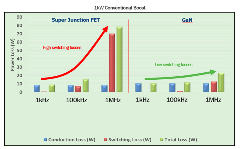
Figure 1: GaN optimized for fast switching
As silicon-based technology approaches its evolutionary limits, design engineers are now looking to wide bandgap technologies such as gallium nitride (GaN) to provide a solution.
Unusually for a new technology, GaN is inherently lower cost than the technology it will supercede, namely silicon. GaN devices are produced in the same factories as silicon devices, using the same manufacturing procedures. So, as GaN devices are smaller than the equivalent silicon device, more can be produced per wafer, thereby lowering the individual cost of each one.
GaN has a number of performance advantages including an electron mobility that is far greater than that of silicon (3.4eV vs. 1.1eV) which gives it the potential to conduct electrons more than 1000 times more efficiently than silicon. Significantly, the gate charge (QG) is lower with GaN and, as this has to be replenished during every switching cycle, GaN is able to be operated at frequencies up to 1 MHz without efficiency degradation while silicon struggles above 100 kHz. Also, unlike silicon, GaN has no body diode and its 2DEG at the AlGaN / GaN boundary surface can conduct current in the reverse direction (known as ‘third quadrant’ operation). As a result, there is no reverse recovery charge (QRR) with GaN, making it ideal for hard switching applications.
GaN does have limited avalanche capability and is more sensitive to overvoltage than silicon, so is ideal in half-bridge topologies where the drain-source voltage (VDS) is clamped to the rail voltage. The lack of a body diode makes GaN a good choice for hard switching totem pole PFC and GaN is also well suited to use in zero-voltage-switching (ZVS) applications, including resonant LLC and active clamp Flyback.
Fast charging adapters at power levels around 45 W to 65 W will benefit from GaN-based active clamp Flyback, while LLC-based GaN is being adopted in 150 W to 300 W power adapters for high-end notebooks, such as those intended for gaming. In these applications, the use of GaN technology doubles the power density, making the adapters both smaller and lighter. In particular, associated magnetic components are able to be reduced in size. For example, the power transformer core can be reduced from an RM10 to an RM8 low profile or planar design. In many applications, the power density is thus doubled or even tripled, making power densities of 30 W/in3 achievable.
In higher power applications, such as power supplies intended to power servers, the cloud and telecom systems, especially those based upon a totem pole PFC, GaN is enabling efficiencies in excess of 99%. This allows these systems to meet the all-important (and rigorous) efficiency standards such as 80+ titanium.
The method used to drive GaN devices is critical to protect the relatively sensitive gate oxide. It is especially important to provide a precisely regulated gate drive amplitude during the time the device is turned ON. One means of achieving this is to add an LDO to an existing silicon MOSFET gate driver. However, this can compromise the gate drive performance so, using a half bridge driver designed specifically for the purpose of powering GaN is preferred.
More specifically, the typical propagation delay time for a silicon MOSFET driver is around 100 ns which is not suitable for driving GaN devices at speeds between 500 kHz and 1 MHz. For speeds such as these, the propagation delay should ideally be no more than 50 ns.
Due to the lower capacitances, a high voltage slew rate can be seen between the drain and source on GaN devices. This can lead to premature, even catastrophic, failure of the device – especially in high power applications. To prevent this, high levels of dv/dt immunity (in the region of 100 V/ns) are necessary.
The PCB can have a material effect on performance in GaN designs, so techniques commonly use in RF-type layouts are often used. It is also advised to use low inductance packages (such as PQFN) for the gate driver.
ON Semiconductor’s NCP51820 is the industry’s first half bridge gate driver that is specifically designed for use with GaN technology. It features a regulated 5.2 V gate drive with a typical propagation delay of just 25 ns. It has dv/dt immunity up to 200 V/ns and is available in a low inductance PQFN style package.

Click image to enlarge
Figure 2: NCP51820 High Performance, 650 V Half Bridge Gate Driver for GaN Power Switches
The growth and adoption for GaN technology will initially come from applications such as the lower power fast charging USB PD power adapters and higher power adapters for gaming laptops. This is primarily due to the availability of controllers and drivers to support these applications that require high switching frequencies, thereby reducing design cycle times. As suitable drivers, controllers and module solutions become available for higher power applications such as servers, the cloud and telecom, then GaN will also see adoption there.


.jpeg)