Author:
Philip Zuk, Vice President of Worldwide Technical Marketing and North American Sales, Transphorm
Date
03/02/2020
 PDF
PDF
Click image to enlarge
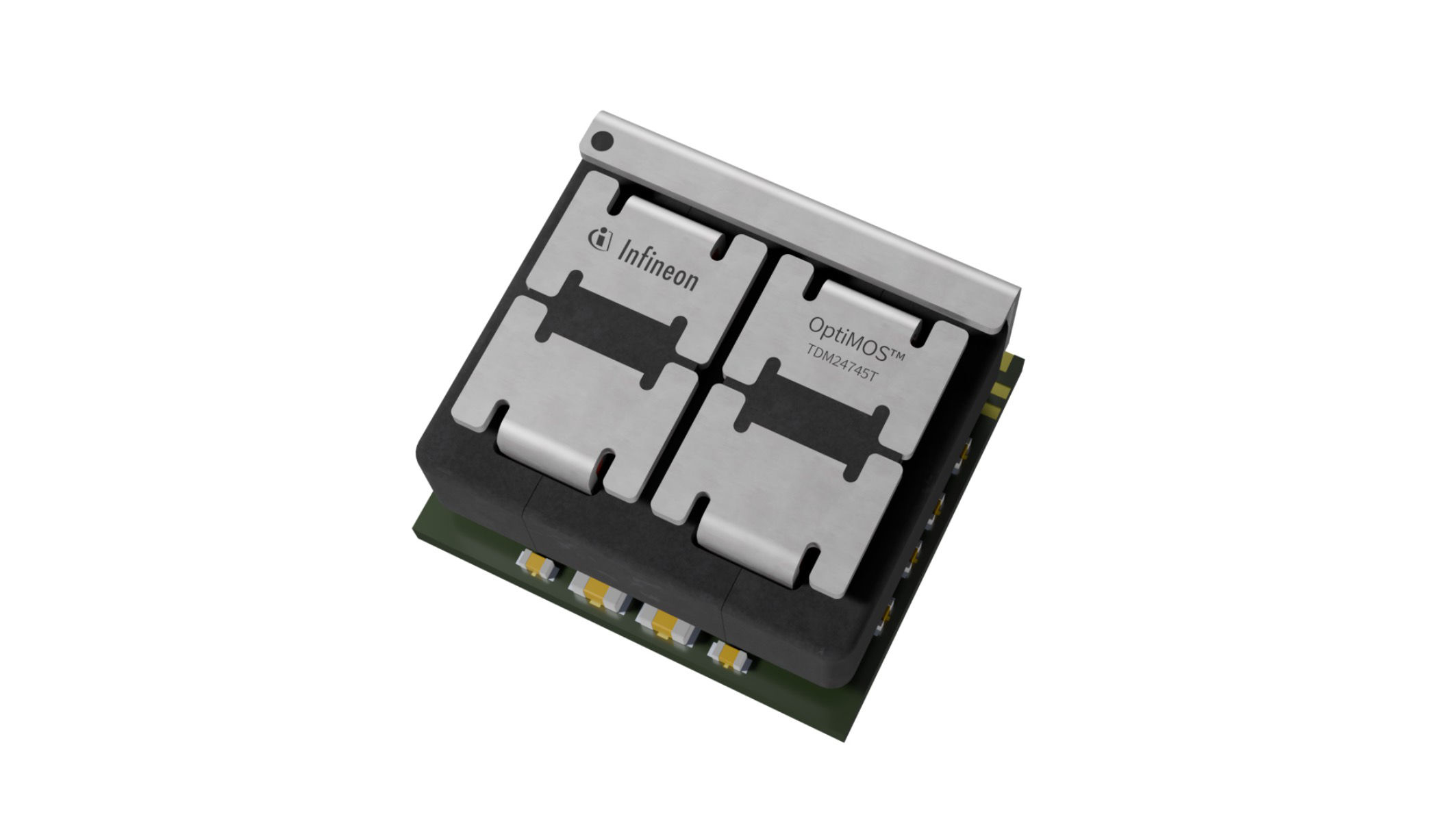
Figure 1: Two-chip normally-off high voltage GaN FET
Two-chip normally-off Gallium Nitride (GaN) FETs are currently used in in-production power systems in various markets ranging from Consumer Adapters, PC Gaming to Broad Industrial. Within these applications, the GaN devices regularly demonstrate the end-to-end benefits expected from GaN, including increased efficiency, higher power output, smaller form factors, and lower overall system costs. Given this, GaN is proving to be a viable alternative to Silicon given its ability to exceed Silicon’s power density and overall system cost limitations. However, while it is true that GaN switches are not drop-in-replacements for Silicon devices, the design techniques required to optimize GaN FETs are not as sensitive and complex as some would suggest. Two-chip normally-off GaN FETs offer simple designability, eliminating the need for many external passive devices to properly drive and protect the gate along with carefully designed PCB layouts notably required by enhancement mode (e-mode) GaN HEMTs.
Concerns when designing with GaN often stem from assumptions that all GaN is alike. It is not. For example, it has been reported that high voltage GaN devices offer a low maximum gate voltage of < 10 V when more than 5 V is required for full channel conduction, a less than ideal rating when compared to the +/- 30 V currently offered by Silicon MOSFETs. A critical point to note is that the GaN referenced here is specifically e-mode GaN. This is not true of all GaN. Today’s leading two-chip normally-off GaN devices pair a state-of-the-art high voltage GaN HEMT with a low voltage Silicon MOSFET. As a result, they offer quieter switching with an additional 8 V resulting in a +/- 20 V gate robustness.
Similarly, it has been reported that high voltage GaN’s turn on threshold (VGTH) rates ~1.5V. Again, this is suboptimal and can pose some undesired design challenges when compared to a Si MOSFET’s threshold of 3.5 V to 4.0 V (typical). However, as with the gate robustness rating, this threshold voltage is not standard across all available GaN technologies. In fact, in-production two-chip normally-off GaN solutions were designed to compete directly with high voltage Silicon superjunction technology. Unlike its e-mode competitor, this GaN does not require a negative gate drive. Additionally, it offers a 4 V threshold—at worst case matching that of the standard superjunction rating.
Another area in which two-chip normally-off GaN FETs differ from e-mode GaN devices is that the external gate drive does not have to be managed in order to guarantee gate reliability. Using a low-voltage MOSFET to drive the two-chip normally-off GaN HEMT results in the market’s most robust gate solution (+/- 20 V) regardless of which gate drive or circuit is used.
When assessing power semiconductor performance, it is also common to look for avalanche ratings. Due to its natural structure, GaN in general does not offer avalanche protection. Instead, it offers a high voltage transient specification, which is higher than a traditional Si avalanche rating (typically 10% more than rated) so the part does not enter an avalanche condition. To that end, the leading two-chip normally-off GaN solution currently offers an 800 V spike rating (V(TR)DSS), which—when using Transphorm GaN FETs—is a repetitive rating that adds to the high reliability confidence in the technology.

Click image to enlarge
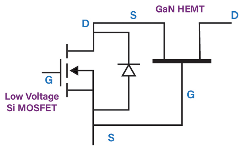
Figure 2: Recommended values for two-chip normally off GaN FET use
Use of the low-voltage MOSFET with the GaN HEMT gives the two-chip normally-off GaN platform still more advantages. For example, with e-mode devices, it is assumed that the switches are truly off with a VGSof 0. However, it is reported that even with custom designed drivers, 0 V may not be enough to guarantee that an e-mode GaN FET is turned off. This is due to the di/dt generated by the gate drive loop. To manage this, e-mode devices require a negative gate drive to guarantee that the e-mode GaN FET is fully off. Use of a negative gate drive can complicate the circuit design, add additional components taking up precious PCB real estate, and add additional cost. It calls for careful consideration of the board layout as well as the implementation of Kelvin source connection, which is required to help protect the gate of the e-mode current controlled device during regular operation. Alternatively, two-chip normally-off GaN being a voltage controlled device along with a 4 V threshold is only required to switch down to 0 V such as a high voltage superjunction device, reaching a true VGSof 0 when off without the use of a negative gate drive or a Kelvin source.
Other key differences between the two different GaN types exist that should be considered. Recent reports indicate that typical e-mode GaN devices must be driven to a gate voltage (VG(ON))rating of ~+5.2 V to fully enhance the channel and achieve the fastest switching possible. Yet, when driving to this speed, the gate drive voltage swing ultimately becomes wide due to the negative value (typically -3 V) required to keep the device off during normal switching operation. This occurrence changes the +5.2 V to +8.2 V (voltage drop in the reverse (3rd quadrant) operation or when used as a free-wheeling diode (FWD)) resulting in additional reverse conduction losses. However, such a gate drive power penalty can be avoided with the use of a two-chip normally off GaN FET—which includes the drop across the low-voltage MOSFET body diode (Vs ~ 0.9 V) plus the IR drop across the channel of the HEMT because it is not required to be driven negative. This can result in a 4x lower loss during that part of the switching cycle.
Lastly, unlike e-mode, two-chip normally-off GaN allows for the use of standard TO-220/TO-247 packages. This allows for a multiple kilowatt design with a single pair of devices without having to parallel—which increases reliability, reduces cost, and still results in a design reaching >99% efficiency in a totem-pole or half bridge topology.
GaN’s ultimate promise is to deliver greater power density at lower overall system costs. Given GaN’s inherent capabilities as well as advantages specific to two-chip normally-off GaN, system designers can expect to fully realize this promise when using GaN in the optimal topology: the bridgeless totem-pole PFC. However, this is not to say that power systems using other topologies do not benefit from GaN.
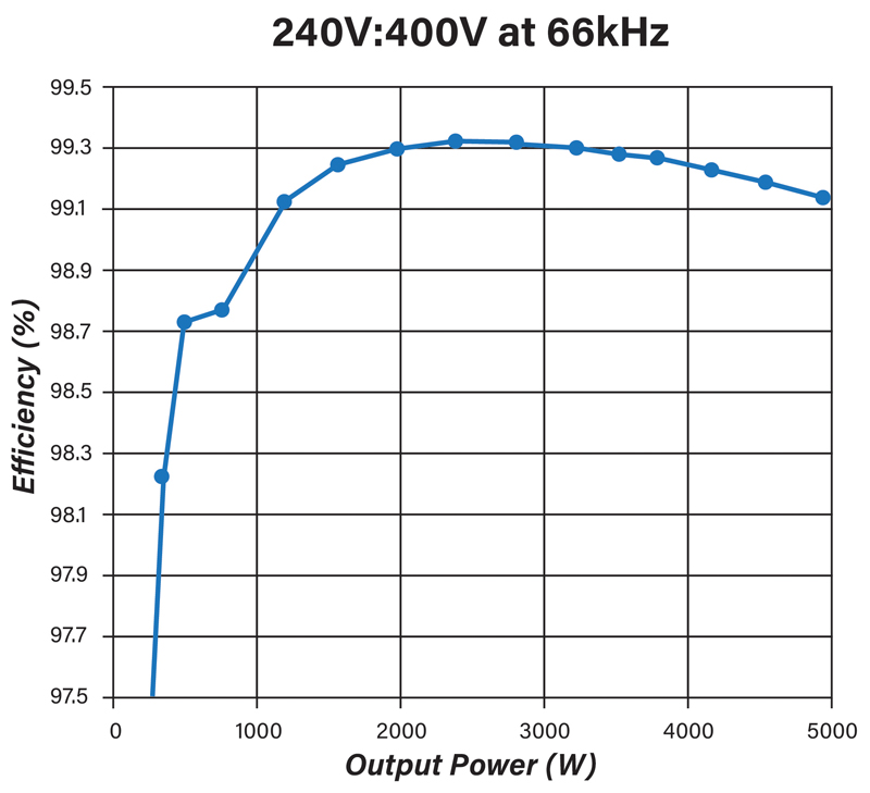
Click image to enlarge
Figure 3: Synchronous boost half-bridge efficiency
To date, in production power applications have used various designs such as standard CCM PFC boost and topologies using the half-bridge structure as a building block (totem-pole, LLC, full bridge (FB), etc.)—all demonstrating various GaN advantages. In fact, high voltage GaN is currently infiltrating the USB type-C PD adapter market—an industry typically relying on the standard single FET Quasi-resonant Flyback (QRF) or the two device active clamp flyback (ACFB) topology. The reason for this adoption trend is simply size reduction. Even a 0.5% decrease in efficiency can raise internal temperatures by 15-20°C, but with GaN’s increased switching speed and lower crossover losses, that thermal impact is eliminated.
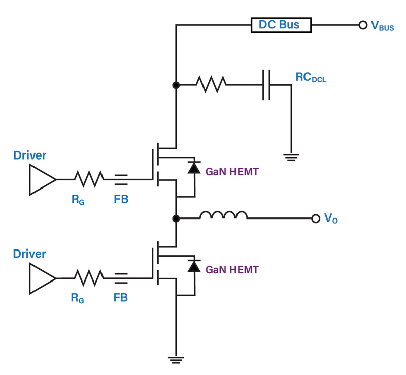
Click image to enlarge
Figure 4: Simplified half-bridge schematic with two-chip normally-off GaN FET