Improving low-voltage DC/DC converter performance with GaN transistors
The emergence of commercially available and cost-effective gallium nitride (GaN) power transistors begins a new age in power electronics. There are significant benefits in using enhancement-mode gallium nitride FET (eGaN FET) devices in power converters for existing data center and telecommunications architectures centering around an input voltage of 48 VDC with load voltages as low as 1 VDC. High-performance GaN power transistors can enable new approaches to power data center and telecommunications systems with higher efficiency and higher power density than possible with previous Si MOSFET based architectures.
Why Focus on Low Voltage?
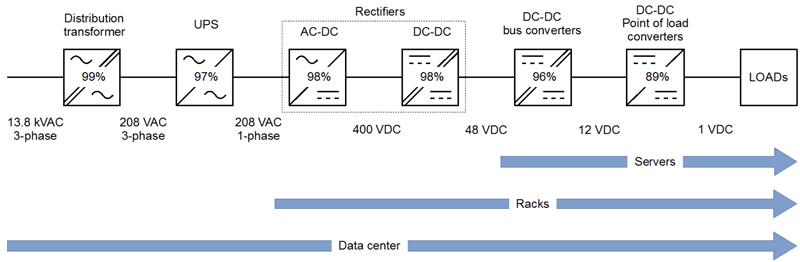
What is the motivation for a focus on lower voltage power? There are two main reasons. First, at the lowest voltage, power conversion touches information processing directly. This connection forces a stringent set of performance requirements on the power electronics that is particularly challenging, especially on size, power density, and transient response. The second reason is that most of the conversion loss is at low voltage, and the lower one goes, the worse it gets. This is shown in Figure 1.
Click image to enlarge
Figure 1: Block diagram of data center power system
Losses at the low voltage stages of the system dominate the overall losses. At higher voltage and power, higher efficiencies are already common, so there is less room for improvement. Thus, while advanced technology may reduce cost or improve power density at the high-voltage and high-power part of the system, there are limited energy savings to be had. On the other hand, advances at the low voltage end can have a large benefit on power density, cost, and efficiency. Also, increased low-voltage efficiency propagates all the way through the system, reducing power requirements for the upstream power components and their associated loss and cost.
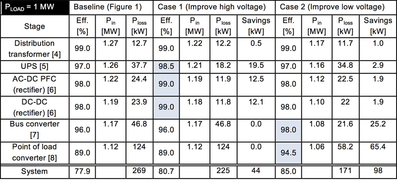
Table I provides some numerical evidence. Consider the system of Figure 1 as our baseline, and assume total load power of 1 MW. For Case 1, we improve the high-voltage power electronics, namely the UPS and the rectifiers, by cutting the relative loss in half. This cuts the total data center losses by 45 kW, or 17%. For Case 2, the losses of the Intermediate Bus Converter (IBC) and the Point-of-Load (POL) converter are cut in half, for a savings of 98 kW – more than 36%. Thus, improvements in the two lowest voltage stages have far more impact than from improvements in the three upstream stages of higher voltage converters.
Clcik image to enlarge
Table I: Power requirements for notional data center power system of Figure 1 with a final load power of 1 MW. Case 1 cuts relative losses of higher voltage power electronics by half, and Case 2 does the same for the low voltage power electronics. Modified efficiencies are shaded for each case
Having identified the largest area for energy savings, we now focus on how to improve the system efficiency from 48 VIN to load voltage. There have been many advances in low voltage power architectures over the years and currently, the most widely adopted architecture is the Intermediate Bus Architecture (IBA), shown in Figure 2. Let’s focus on an IBA with nominal DC bus voltages centering around 48 VIN and 12 VIN.

Click image to enlarge
Figure 2: Intermediate Bus Architecture (IBA)
eGaN FET-based 48 VIN bus converter performance
The 48 VIN IBC is a key component of typical server power distribution systems. In a typical intermediate bus architecture, standard “brick” format DC-DC IBCs provide isolation and voltage step-down. In a data processing system, power processing is considered a cost, and data processing a source of profit. Hence, there is great pressure to increase power density and free up more board real estate for data processing.
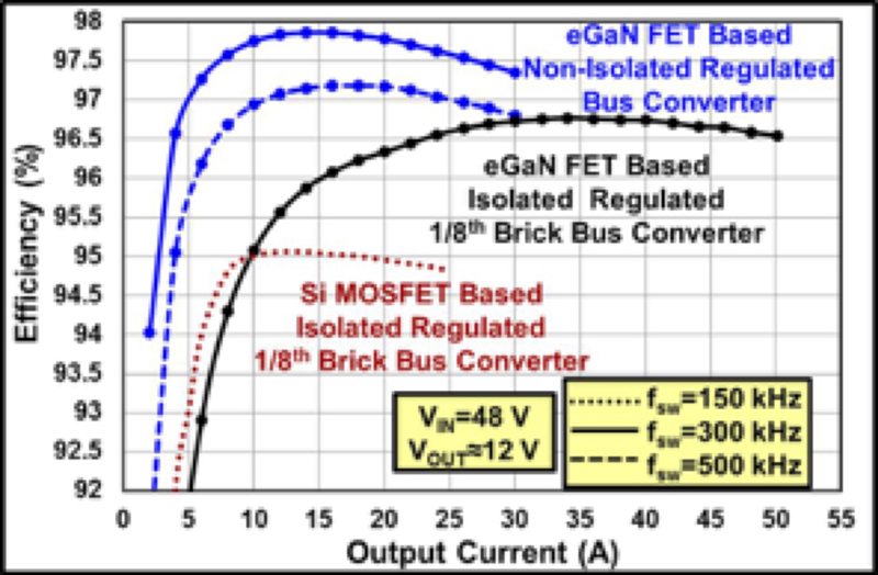
GaN transistors, offering lower on-resistance, faster switching speeds, higher thermal conductivity, and smaller size than their aging Si MOSFET predecessors enable an increase in efficiency, power density, and output power handling capability, reducing the resources required for power management. Shown in red in Figure 3 is the efficiency of a state-of-the-art regulated Si MOSFET based eighth-brick IBC.
Click image to enlarge
Figure 3: Efficiency comparison of eGaN FET and Si MOSFET based isolated eighth brick converters and a non-isolated GaN-based IBC buck converter
The electrical and thermal performance of Si MOSFETs limit the Si-based solution to a switching frequency of 150 kHz and maximum output power of 300 W. For comparison, the efficiency of an eGaN FET-based eighth brick regulated IBC, occupying the same area, is also shown in Figure 3 in black. Utilizing the superior electrical and thermal performance of eGaN FETs, an increased output power of 500 W can be realized at twice the switching frequency, 300 kHz.
With eGaN FETs capable of efficiently switching higher power levels at higher frequencies, system designers, who are always under constant pressure to increase efficiency and power density, as well as reduce cost, can consider non-isolated IBC approaches. Non-isolated buck IBCs, with efficiency shown in blue in Figure 3 for switching frequencies of 300 kHz and 500 kHz, are capable of higher efficiencies and higher frequencies than traditional isolated IBC brick approaches and enabled by more efficient GaN power transistors.
eGaN FET-based 12 VIN Point-of-Load converter performance
Non-isolated point-of-load (POL) buck converters are found in a wide range of applications requiring a step-down voltage conversion. High-current 12 VIN-to load POL buck converters are ubiquitous in server and data processing systems. With the ever-increasing power demands of computing and telecom systems and the desire for smaller size and lower power consumption, POL converters achieving higher power density and efficiency are a necessity.
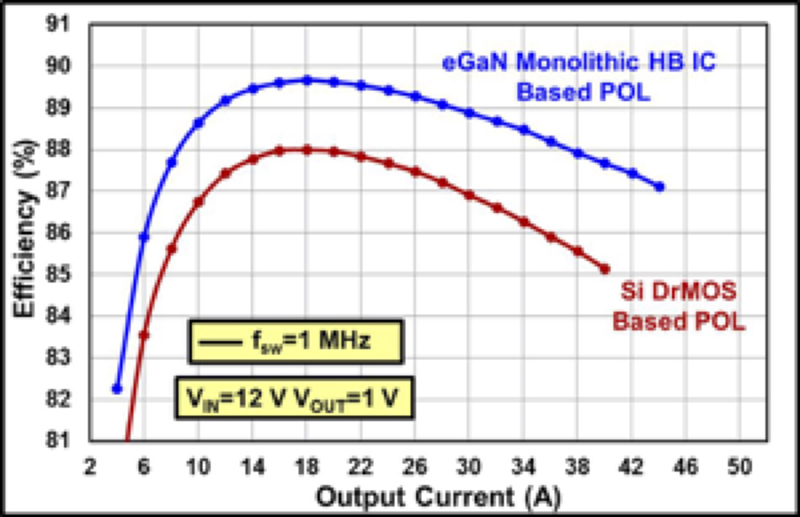
The total system efficiency of eGaN FET and Si DrMOS-based 12 VIN to 1 VOUT buck converters operated at a switching frequency of 1 MHz are shown in Figure 4. This includes losses of the entire system, including the inductor, capacitors, and PCB losses. The eGaN monolithic half bridge (HB) IC based POL buck converter efficiency is higher than the Si DrMOS based solution at every operating point. At a light load condition of 10 A, the eGaN FET based design has an over 1.5% efficiency advantage. At a heavy load condition of 40 A, the efficiency advantage is around 2.5%, which translates to an almost 20% reduction in total system power loss.
Click image to enlarge
Figure 4: Efficiency comparison between eGaN FET and Si MOSFET based buck POL converters
Enabling single-stage 48 VIN Point-of-Load with GaN
When the state-of-the-art intermediate bus architecture (IBA) of Figure 2 was first introduced, the benefits of replacing a single power conversion stage (distributed power architecture) with two power conversion stages to improve system performance were not readily apparent. But, as the number of load voltages increased, and the load demands became more complex, the architecture provided better performance and lower system cost with its divide-and-conquer approach.
Since the adoption of the IBA, the power demands of data and telecom systems have continued to increase and, with emerging trends like cloud computing, the system power demands show no signs of slowing down. Bus converters are currently approaching about an order of magnitude increase in output power since the adoption of the IBA, from around 100 W to current designs of around 1 kW in a quarter brick footprint. This means that the amount of current on the 12 V bus to the POL converters has also increased by a factor of 10 and, without reductions in busing resistance, a two orders of magnitude increase in busing conduction losses follows.
Recent developments in placing high frequency buck regulators directly on the microprocessor is further changing the way power is delivered to CPUs. The 48 VIN-to-12 VOUT IBC remains unchanged, but now the 12 VIN POL converter, which was previously used to directly power the CPU, now serves as a second IBC stage and the dynamically regulated POL conversion is done at the microprocessor level from 1.8 VIN-to-load. With the new 1.8 V bus, the architecture has grown to three power conversion stages. With the increasing conversion losses in the 48 VIN bus converter, mounting 12 V busing losses on the motherboards, and a redundant second 12 VIN IBC conversion stage, alternative architectures are now being considered.
A potential solution with lower cost, greater simplicity, and higher performance is a non-isolated IBC converter from 48 VIN to 1.8 VOUT. A comparison of estimated efficiencies and power densities for the two stage 48 VIN to 1.8 VOUT non-isolated IBA, and the traditional three stage IBA approach using GaN-based designs is shown in Figure 5 and summarized in Table II. The total system efficiency of the direct 48 VIN to 1.8 VOUT conversion approach is around 0.5% higher, and the estimated power density has been improved by more than 65% compared with the conventional three stage IBA. There is a clear cost and power density advantage by removing one of the redundant bus conversion stages, and by having a single GaN-based bus converter from 48 VIN to 1.8 VOUT.

Click image to enlarge
Figure 5: Performance comparisons of 48 VIN three stage and two stage non-isolated intermediate bus architectures
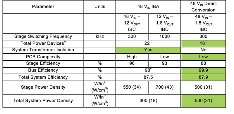
Table II: Summary of 48 VIN three stage and two stage non-isolated intermediate bus architecture performance comparisons
A look back and ahead
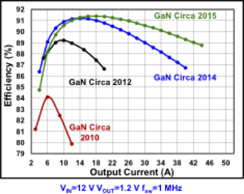
There are immediate benefits of enhancement-mode gallium nitride FETs (eGaN FETs) in both existing and potential new data center and telecommunications power architectures with an input voltage range centered around 48 VDC and with load voltage as low as 1 VDC were demonstrated. As GaN technology advances and adoption increases, the improvement will continue to increase. Using the application of eGaN FETs in 12 VIN POL converters as an example, the rapid progression of GaN performance is shown in Figure 6.
Click image to enlarge
Figure 6: Evolution of performance for GaN transistor based 12 VIN POL converters
GaN transistors have exhibited exceptional device characteristics since their inception. However, initial (circa 2010) in-circuit performance was limited by an insufficient understanding of the nuances of designing with this new technology. Enhancement-mode GaN transistors operate much like their MOSFET predecessors, with a few key intrinsic differences.
Through the development of improved design basics and GaN specific ICs, GaN-based designs began to realize their in-circuit performance potential (circa 2012). With the rapid maturation in GaN device technology and the continued improvement of design fundamentals, the in-circuit performance continued to improve (circa 2014). With new technological breakthroughs, such as monolithic integration, GaN transistors again raised the bar for high frequency power conversion performance (circa 2015).
As this relatively new technology continues to rapidly improve, the supporting GaN ecosystem continues to grow, and circuit designers continue to improve application understanding better utilizing this more capable technology, GaN-based power converters will continue to widen the performance gap over their MOSFET predecessors. This will enable new levels of performance achievable in existing applications, as well enabling new applications and new approaches to existing applications. The journey is just beginning.