SiC FETs can be considered for renewable energy power conversion applications, giving better efficiency and savings in system size, weight and cost
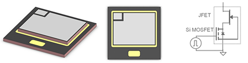
Figure 1: The stacked SiC FET cascode with an Si-MOSFET die on the source pad of a SiC JFET and its equivalent circuit
Initiatives to go 'carbon' neutral' such as the '2050 long-term strategy' in the EU, to achieve net-zero greenhouse gas emissions, have sharpened engineers' focus on power conversion architectures and their efficiency. Minimising losses has always been a design engineer's goal anyway; low values directly reduce energy and cooling costs while equipment can be smaller, cheaper, lighter, cooler and more reliable. With renewable energy sources still relatively expensive compared with fossil fuel, avoiding power conversion losses is now an imperative.
Semiconductor switches are key to conversion efficiency
Whatever the renewable energy source, ultimately what's needed for distribution is an AC line voltage. Inverters generate line AC from a DC source or 'link' which may be directly from PV panels, batteries or rectified AC at higher or lower voltage. Power factor correction stages switch AC lines and boost to DC levels while forcing line current to follow line voltage, and downstream equipment AC-DC and DC-DC converters generate the final voltages. In each case, semiconductor switches are employed of different types depending on the application. IGBTs have been used typically at high power and voltages, with Silicon MOSFETs common for downstream power stages.
Switches are never perfect though, and produce on-state and switching losses, so IGBT and MOSFET technologies are being continually refined for better performance. However, renewable energy power conversion must be scaled to higher and higher currents and voltages to be viable, and this has exposed limits to IGBT and Si-MOSFET performance, in turn limiting conversion efficiency economically achievable.
Wide band-gap switches - a breakthrough technology, but...
Wide band-gap switches fabricated in Silicon Carbide (SiC) and Gallium Nitride (GaN) have become mainstream with their ability to switch dramatically faster than IGBTs and somewhat faster than MOSFETs, reducing dynamic losses. Initial commercial devices were very expensive, needed very particular gate drive, had uncompetitive on-resistance and in some parameters such as avalanche ratings, were inferior to Si-MOSFETs. Reliability was unproven with some failure mechanisms poorly understood. However, the fast switching frequencies possible spurred development of the technologies, as knock-on advantages could also be seen such as the reduction in cost and size of associated passive components, particularly magnetics.
SiC and GaN device specifications have now advanced, costs have fallen and reliability demonstrated but there is still a discernible gap between real performance and the ideal switch; one that is easy to drive with lowest on-resistance and switching loss.
SiC FETs - closer to the ideal switch
A simple JFET fabricated in SiC is close to the ideal switch except for an important limitation; it is normally ON at zero gate voltage. This can be an advantage in applications such as circuit protection but in power converters, it risks disastrous shoot-through under transient conditions and start-up/shut-down. A solution has been known about for decades - the stacked cascode. Originally invented for vacuum tubes, it has resurfaced as a combination of a low-voltage Si-MOSFET and high-voltage SiC JFET (Figure 1) which is normally OFF and has an easy Si-MOSFET gate drive, but still has the advantages of SiC; high critical breakdown voltage, low on-resistance, low switching loss and high temperature rating. Avalanche and short-circuit current limiting are also inherent. Physically, the Si-MOSFET can be stacked on the SiC JFET die and packaged discretely in TO-247 format for example, or incorporated into modules.
The Si-MOSFET is in series with the conduction path but as it need only be a low voltage type, around 25V rating, it can have an insignificant on-resistance of less than one milliohm. An example SiC FET part is the UF3SC120009 device from UnitedSiC which is rated at 1200V with an overall on-resistance of 8.6 milliohms. It is available as a die for modules and also in the four-lead TO-247-4L package which incorporates a Kelvin source connection, vital when operating at the high edge rates possible with SiC.
Key SiC FET features
It's instructive to review some of the key features of the SiC FET in comparison with the alternatives; IGBTs, Si-MOSFETs, SiC MOSFETs and GaN HEMTs. Usability is a major plus; the gate of the SiC FET has a threshold of around 5V and is stable with operating conditions and temperature. Protection diodes are included that clamp at +/-25V so a 'standard' gate drive of 0-12V is possible making the parts backward compatible with Si-MOSFETs and IGBTs. In comparison, SiC MOSFETs and GaN devices particularly, have limited allowed gate voltage swing with recommended operating values uncomfortably close to absolute maximums.
On-resistance is obviously key to low loss and should be compared between devices at a particular voltage rating - parts in the UF3SC range have the lowest available RDSON in TO-247 packages of any device type. On-resistance per unit die area, RDSA, for a particular voltage rating is also an important figure of merit, as a low value indicates high yield from wafers and hence potentially lower cost. It also signifies that low on-resistance can be achieved with small die which in turn have low device capacitances and consequent faster switching and low loss.
How RDSON varies with temperature is also important, with SiC FETs performing particularly well; the 650V UF3SC065007K4S from UnitedSiC for example, at 125-150°C has a conduction loss 2.5 x to 4x lower than the best 650V superjunction Si-MOSFETs currently available and the rate of increase of RDSON in SiC FETs is comparable with SiC MOSFETs.
Switching losses are dependent on device capacitances that have to be charged and discharged each cycle, dissipating power and affecting edge rates. SiC FETs exhibit very low charge or QRR values associated with the device capacitances, superjunction MOSFET QRR for example can be 10 - 50x higher and have dV/dt limitations under hard recovery.
In some applications, commutation or reverse conduction occurs in switches such as in motor drives. To allow this, IGBTs require parallel fast diodes. Si-and SiC-MOSFETs have an integral body diode but with high forward voltage drop. SiC FETs like GaN do not have a body diode but conduct through the channel in reverse with low loss and very low recovery charge.
Channel conduction in SiC FETs also occurs when voltage ratings are exceeded giving an avalanche effect which can handle several joules of energy and protect the device. GaN has no similar effect. Short circuit over-currents also self-limit as the JFET on-resistance increases with temperature, reducing peak current. The same temperature dependence allows SiC FETs to be easily paralleled with excellent static and dynamic sharing, enhanced by the insensitivity of gate threshold to temperature change.
SiC FETS in renewable energy applications
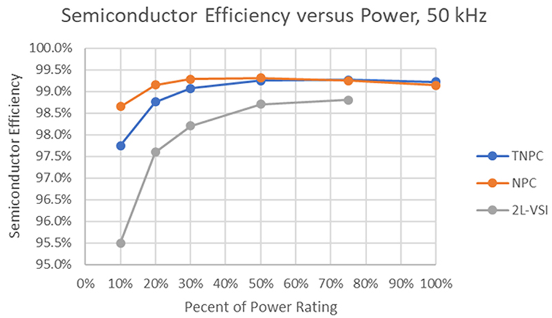
PV inverters are a prime candidate for better switches; panel conversion efficiency from incident solar energy to DC produced is already low, so it is important that the power conversion to AC line is as efficient as possible. Panels are placed electrically in series for high voltages so currents are lower for a given power, so a high-power solar inverter typically might need to operate from 800V to produce 480VAC for distribution. IGBTs have been used traditionally but have to switch at just a few kHz due to their speed limitation meaning large filter magnetics. Si-MOSFETs have high conduction losses at high power and GaN is not suitable for 800V. SiC FETs however are a real alternative. UnitedSiC has calculated efficiency achievable for a 60kVA, 480VAC inverter operating from 800V at different frequencies and using different topologies; 2-level, NPC and TNPC (Figure 3). At 50kHz, the 2-level circuit uses just 6 UF3SC120009K4S devices for a peak of 98.8% efficiency at a limiting 45kVA load but a TNPC circuit enables full 60kVA output. It uses a total of 12 devices but gains an extra 1% in efficiency, representing about 600W of saved power loss, and discrete TO-247 devices can be employed rather than expensive IGBT modules. The extra gate drives needed are a small overhead as they are simple and consume little power. Operation at 50kHz allows the use of much smaller output filters with consequent additional efficiency, size and cost savings and if the frequency is kept to the IGBT range of around 10kHz, losses in the switches reduce still further.
Click image to enlarge
Figure 2: Calculated efficiency for a 60kVA, 800VDC - 480VAC solar inverter using SiC FETS and different conversion topologies
Conclusion
SiC FETs are the closest yet to an ideal switch and with die and discrete package options, can be used as retrospective upgrades to IGBTs and Si-MOSFETs as well as in new designs. With their high voltage and current ratings SiC FETs can be seriously considered for use in all renewable energy power conversion applications for better efficiency and consequent savings in system size, weight and cost. Those greenhouse gas emissions targets get a little easier to achieve as well.