Flat sheets of graphite just one carbon atom thick, called graphene, display unique optical and electronic properties for use in future devices. In particular, graphene is nearly transparent to light and other electromagnetic (EM) waves, making it useful for liquid crystal displays and light-emitting diodes. However, some researchers want to make graphene absorb more EM radiation, so that other proposed applications, such as photodetectors and solar cells, can be realized.
A team led by Riichiro Saito at Tohoku University are taking a new approach to this problem, by exploiting the fact that the absorption of a surface depends strongly on the angle of the incident light. They propose sandwiching a single layer of graphene between two different dielectric (insulating) materials. With this setup, the proportions of radiation reflected, absorbed or transmitted by the graphene can be changed by adjusting the angle of incidence of the radiation, the properties of the dielectrics, or the energy of electrons in the graphene.
One of Saito’s students, Muhamad Shoufie Ukhtary, performed theoretical calculations to show that, by carefully choosing the right materials and design, the absorption of microwave radiation (at 10-100 GHz) in their setup could be tuned from values near 0 to almost 100%.
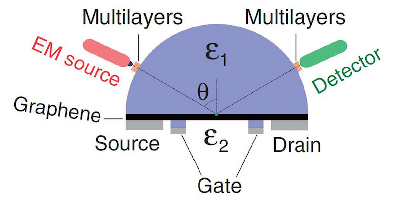
The researchers used this principle to describe a practical EM wave-switching device in which the two dielectrics surrounding the graphene would be silicon and a vacuum, and the electron energy could be tuned using voltage gates (see figure). They are hopeful that an experimental model of this relatively simple design could be built in the near future.
Reference and Affiliation
M. Shoufie Ukhtary1, Eddwi H. Hasdeo1, Ahmad R. T. Nugraha1, and Riichiro Saito1. Fermi energy-dependence of electromagnetic wave absorption in graphene. Applied Physics Express 8, 055102 (2015).
http://dx.doi.org/10.7567/APEX.8.055102
1. Department of Physics, Tohoku University, Sendai 980-8578, Japan
Researchers at Tohoku University have shown that the optical absorption of graphene can be controlled by sandwiching it between two dielectric materials and adjusting the angle of incidence (θ) of the EM radiation. In this proposed device, the dielectrics are silicon (ε1) and a vacuum (ε2), and the energy of electrons in the graphene can be controlled using voltage gates.