Measurements at Berkeley Lab's Molecular Foundry reveal exotic spin properties that could drive new form of data storage
Researchers working at the Department of Energy's Lawrence Berkeley National Laboratory (Berkeley Lab) coupled graphene, a monolayer form of carbon, with thin layers of magnetic materials like cobalt and nickel to produce exotic behavior in electrons that could be useful for next-generation computing applications.
The work was performed in collaboration with French scientists including Nobel Laureate Albert Fert, an emeritus professor at Paris-Sud University and scientific director for a research laboratory in France. The team performed key measurements at Berkeley Lab's Molecular Foundry, a DOE Office of Science User Facility focused on nanoscience research.
Fert shared the Nobel Prize in Physics in 2007 for his work in understanding a magnetic effect in multilayer materials that led to new technology for reading data in hard drives, for example, and gave rise to a new field studying how to exploit and control a fundamental property known as "spin" in electrons to drive a new type of low-energy, high-speed computer memory and logic technology known as spintronics.
In this latest work, published online Monday in the journal Nature Materials, the research team showed how that spin property - analogous to a compass needle that can be tuned to face either north or south - is affected by the interaction of graphene with the magnetic layers.
The researchers found that the material's electronic and magnetic properties create tiny swirling patterns where the layers meet, and this effect gives scientists hope for controlling the direction of these swirls and tapping this effect for a form of spintronics applications known as "spin-orbitronics" in ultrathin materials. The ultimate goal is to quickly and efficiently store and manipulate data at very small scales, and without the heat buildup that is a common hiccup for miniaturizing computing devices.
Typically, researchers working to produce this behavior for electrons in materials have coupled heavy and expensive metals like platinum and tantalum with magnetic materials to achieve such effects, but graphene offers a potentially revolutionary alternative since it is ultrathin, lightweight, has very high electrical conductivity, and can also serve as a protective layer for corrosion-prone magnetic materials.
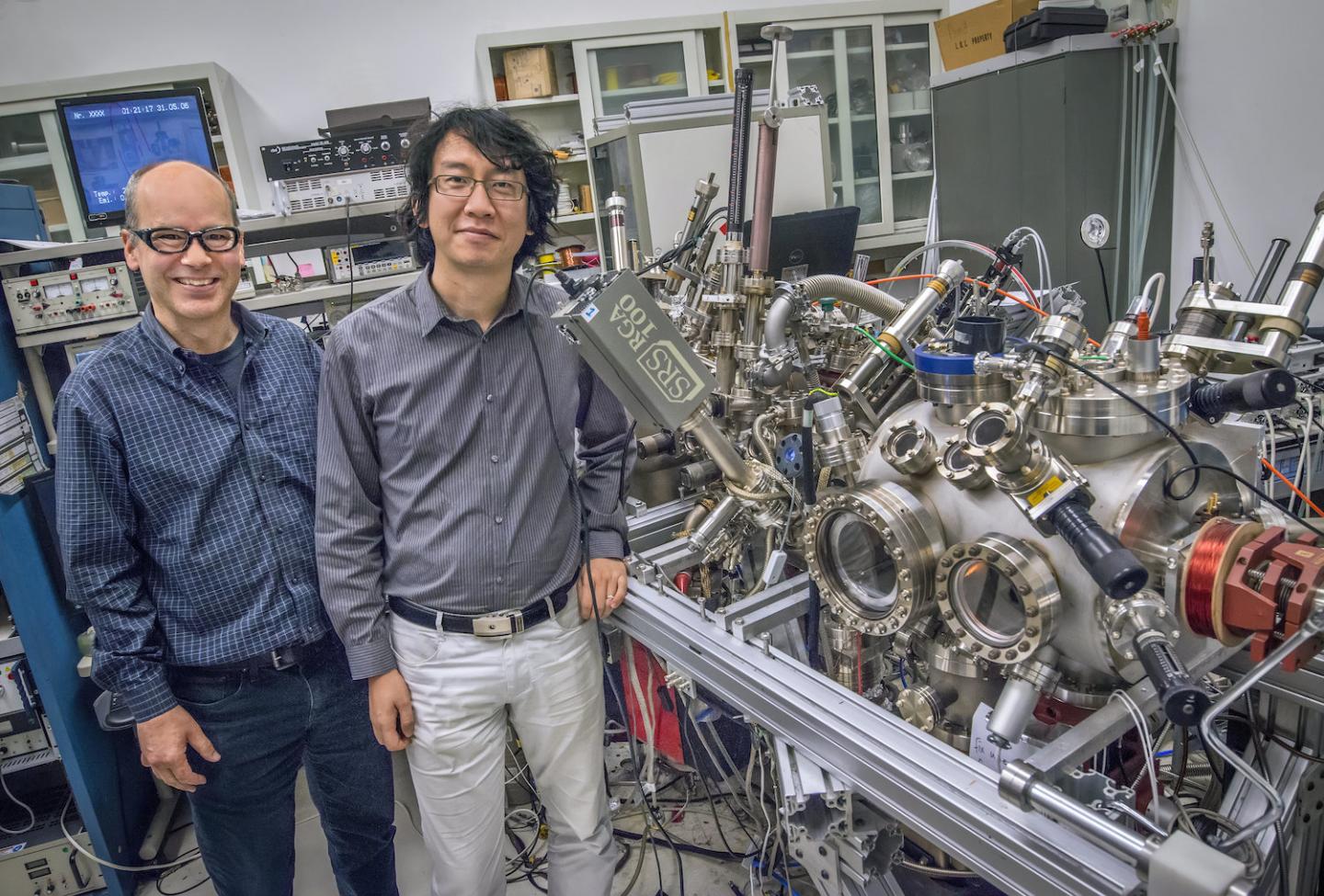
"You could think about replacing computer hard disks with all solid state devices - no moving parts - using electrical signals alone," said Andreas Schmid, a staff scientist at the Molecular Foundry who participated in the research. "Part of the goal is to get lower power-consumption and non-volatile data storage."
The latest research represents an early step toward this goal, Schmid noted, and a next step is to control nanoscale magnetic features, called skyrmions, which can exhibit a property known as chirality that makes them swirl in either a clockwise or counterclockwise direction.
In more conventional layered materials, electrons traveling through the materials can act like an "electron wind" that changes magnetic structures like a pile of leaves blown by a strong wind, Schmid said.
But with the new graphene-layered material, its strong electron spin effects can drive magnetic textures of opposite chirality in different directions as a result of the "spin Hall effect," which explains how electrical currents can affect spin and vice versa. If that chirality can be universally aligned across a material and flipped in a controlled way, researchers could use it to process data.
"Calculations by other team members show that if you take different magnetic materials and graphene and build a multilayer stack of many repeating structures, then this phenomenon and effect could possibly be very powerfully amplified," Schmid said.
To measure the layered material, scientists applied spin-polarized low-energy electron microscopy (SPLEEM) using an instrument at the Molecular Foundry's National Center for Electron Microscopy. It is one of just a handful of specialized devices around the world that allow scientists to combine different images to essentially map the orientations of a sample's 3-D magnetization profile (or vector), revealing a its "spin textures."
The research team also created the samples using the same SPLEEM instrument through a precise process known as molecular beam epitaxy, and separately studied the samples using other forms of electron-beam probing techniques.
Gong Chen, a co-lead author who participated in the study as a postdoctoral researcher at the Molecular Foundry and is now an assistant project scientist in the UC Davis Physics Department, said the collaboration sprang out of a discussion with French scientists at a conference in 2016 - both groups had independently been working on similar research and realized the synergy of working together.
While the effects that researchers have now observed in the latest experiments had been discussed decades ago in previous journal articles, Chen noted that the concept of using an atomically thin material like graphene in place of heavy elements to generate those effects was a new concept.
"It has only recently become a hot topic," Chen said. "This effect in thin films had been ignored for a long time. This type of multilayer stacking is really stable and robust."
Using skyrmions could be revolutionary for data processing, he said, because information can potentially be stored at much higher densities than is possible with conventional technologies, and with much lower power usage.
Molecular Foundry researchers are now working to form the graphene-magnetic multilayer material on an insulator or semiconductor to bring it closer to potential applications, Schmid said.
###
Researchers from Grenoble Alps University; Paris-Sud University; a joint center that includes the French National Center for Scientific Research, Thales Physics Lab, Paris-Sud University, and Paris-Saclay University in France; University of California, Davis; the Chinese Academy of Sciences; Nuclear Technology Development Center (CDTN), Federal University of Minas Gerais, and Federal University de Lavras in Brazil participated in the study.
The work was supported by the U.S. Department of Energy Office of Science; the European Union's Horizon 2020 Research and Innovation Program; the U.S. National Science Foundation; the University of California Office of the President Multicampus Research Programs and Initiatives; Brazil's CAPES, CNPq and FAPEMIG programs; and the 1000 Talents Program for Young Scientists of China and Ningbo Program.
Lawrence Berkeley National Laboratory addresses the world's most urgent scientific challenges by advancing sustainable energy, protecting human health, creating new materials, and revealing the origin and fate of the universe. Founded in 1931, Berkeley Lab's scientific expertise has been recognized with 13 Nobel Prizes. The University of California manages Berkeley Lab for the U.S. Department of Energy's Office of Science. For more, visit http://www.
DOE's Office of Science is the single largest supporter of basic research in the physical sciences in the United States, and is working to address some of the most pressing challenges of our time. For more information, please visit science.energy.gov.
EurekAlert!, the online, global news service operated by AAAS, the science society: https://www.eurekalert.org/pub_releases/2018-05/dbnl-glw052518.php