Half Bridge, Gate Driver Measurements for Wide Bandgap
Tips for tackling the biggest measurement challenge power engineers face: getting the signal from the test point to your scope
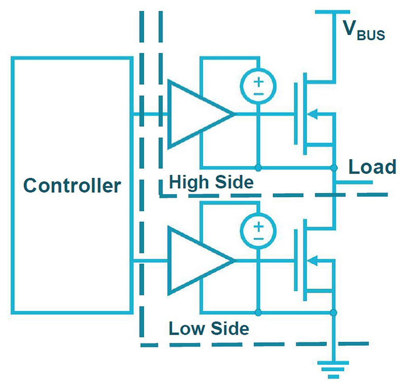
Figure 1. The half-bridge circuit is widely used to convert electrical energy efficiently in modern designs
The faster switching transitions on modern wide bandgap power devices (SiC, GaN) have made measuring and characterizing a considerable challenge, and in some cases, nearly impossible. That is changing with new isolated probing technologies that are allowing designers to at long last confidently measure half bridge and gate driver waveforms that were previously hidden. With a good understanding of the challenges involved, and use of the right probing technologies and techniques, power engineers can more quickly and efficiently characterize and optimize their designs.
The half bridge circuit (Figure 1) is widely used across many applications in the field of power electronics, and is the basic circuit for converting electrical energy efficiently in modern designs. The benefits of this circuit, however, can only be realized when the half bridge, the gate drivers and the layout have all been properly designed and optimized. When measured results do not agree with expected results, it may be difficult to extract meaningful details about the device under test. To make matters worse, waveforms can dramatically change depending on the probe position and other factors, ultimately leaving the designer with more questions than answers.
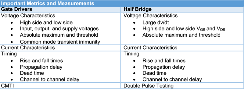
The requirements for efficiency and power densities often vary based on application design requirements, such as whether you’re optimizing for price versus performance. The requirements for improving energy efficiency in power densities will determine the design topology, and in turn the measurement equipment and techniques that should be considered. Table 1 summarizes the most important metrics and measurements for half bridge and gate drivers.
Click image to enlarge
Table 1. These are the most important measurements for gate drivers and half bridge configurations
Accurate power measurements depend on the measurement system’s performance in a number of areas including voltage handling, common mode rejection, connectivity, temperature handling capabilities, and the ability to measure very small current. Despite rapidly changing power design requirements, true advancements in test and measurement have not kept pace. In some cases, designers have been forced to devise custom measurement solutions, or must make do by only approximating certain measurements and missing out on potential optimizations.
At the most basic level, these measurements are performed with an oscilloscope together with an appropriate set of probes. The oscilloscope is rarely an issue when it comes to making accurate and reliable power measurements. Rather, the biggest challenge has become getting the signal from the test point to the scope. As such, it’s critical to select the right probe for the job, whether it’s a passive or single ended probe, traditional high voltage differential probe, a current probe, or an isolated probe.
Single end probes – low side measurements
Most oscilloscopes ship with a set of passive or single ended probes. Such probes can only accurately measure signals that are ground referenced to the scope, limiting them to low side measurements. You can perform high side measurements using passive probes by floating the scope or using a pair of probes to perform pseudo differential measurements as we discuss later, but this is generally not recommended.
When considering how much probe performance is needed for a particular measurement task, there’s a tendency to focus on bandwidth. Conventional thinking holds that higher bandwidth means higher performance. And, to be sure, bandwidth is important as it defines the highest frequency at which the peak-to-peak amplitude of a sine wave can be measured. But the reality is you are not going to be measuring sine waves in the frequency domain. Instead you want to display and measure the signal under consideration over time – in other words in the time domain.
Consequently, the performance metric you should pay closest attention to for half bridge and gate driver measurements is rise time. The rise time can be calculated from bandwidth, but the only way to reliably know the rise time and full time response of a measurement system is to actually measure it with a step signal that is much faster than the signal you’re measuring.
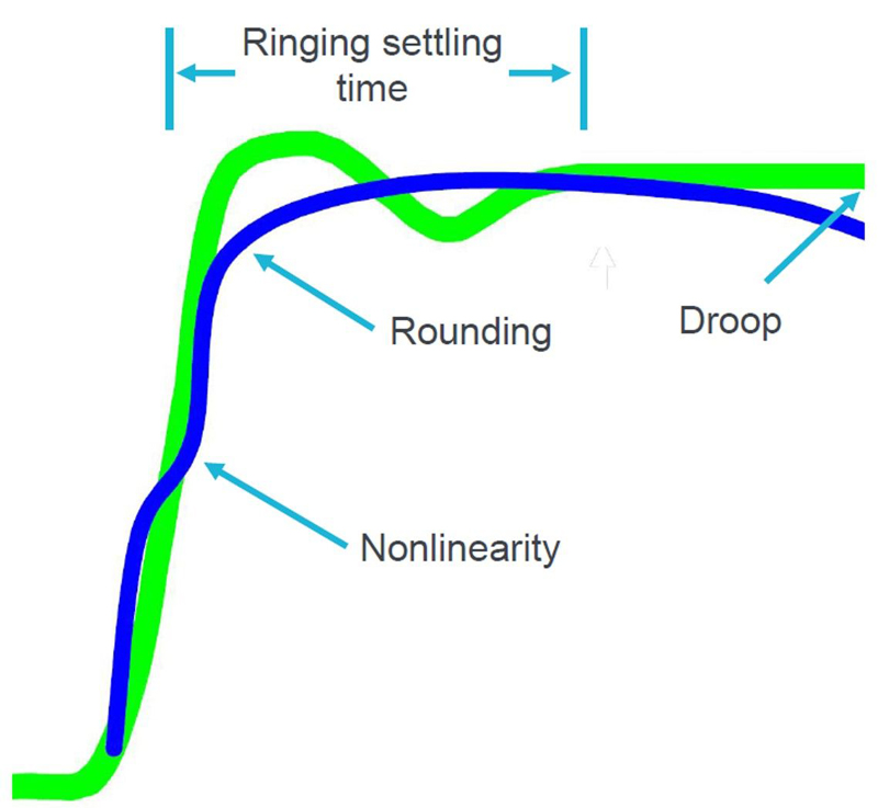
A measurement system with insufficient rise time capabilities will have step response aberrations like those shown in Figure 2 including non-linearity, rounding and drooping. It can be very difficult to know if these aberrations are actually from the measurement system or from the DUT and can only truly be known if you have characterized the measurement system. To avoid these measurement errors, be sure to select a probe with faster rise time than the device you’re testing.
Click image to enlarge
Figure 2. Rise time is a more important factor in power device measurement accuracy than bandwidth
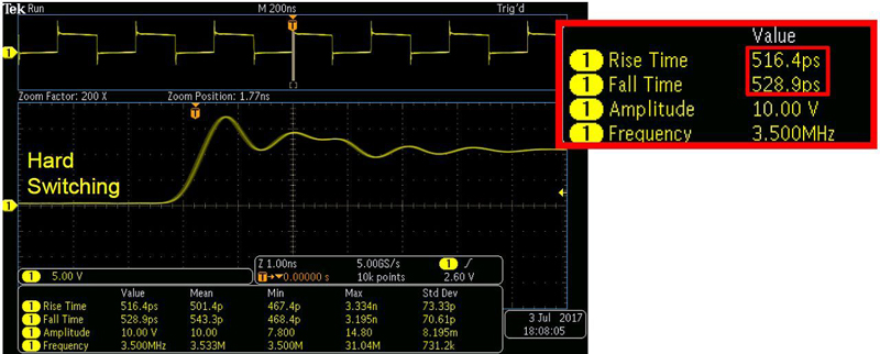
The value of a fast probe is shown in Figure 3 where we used a 1 GHz passive probe to measure the low side of a high-speed FET driver showing < 1 ns rise time on its spec sheet. Because this probe has a rise time specification of around 450 ps, we were able to measure rise time at just over 500 ps. If this measurement was made using a probe with a slower rise time, such as a 500 MHz probe, the high frequency content located at the front corner the waveform would have been rounded off.
Click image to enlarge
Figure 3. A 1 GHz Tektronix TPP1000 passive probe was able to accurately measure a high-speed FET thanks to its 450 ps rise time specification
Measuring gate driver current
When measuring gate driver current, many designers use an external sense resistor instead of a current probe simply because the inductance from the wire loop needed to measure with a current probe influences the circuit. Often, there's a resistor already in the design in series between the gate driver and the gate. To minimize insertion impedance, the resistance of the sense resistor is kept very small, meaning that the voltage drop across the sense resistor is also be very small. Current is calculated by taking the measured value of the voltage drop across the sense resistor and then dividing it by the known resistance of the resistor.
Placing a sense resistor on the low side connection usually means one terminal is at ground. The primary difference between the low side and the high side placement is that low side placement can reduce or effectively eliminate common mode voltage, which appears simultaneously and is in phase on either side of the current sense resistor. For this reason, low side sense resistor placement is typically recommended, especially in high voltage situations. In high current applications, however, ground bounces show up as a common mode signal.
Float the scope
One technique to break ground loops is to “float the scope” or float the circuit being measured. Floating breaks the connection to ground earth so you can theoretically make differential measurements between two test points because the scope ground has been defeated. This practice is inherently dangerous, as it defeats that the protection from electrical shock and can damage the measurement equipment.
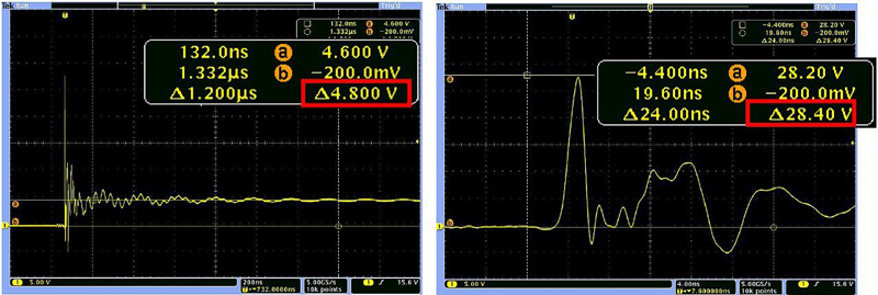
Floating may be useful for some measurements, particularly at very low frequencies, with the caveat that without a low impedance ground connection, radiated and conducted emissions from the scope may interfere with the measurements in the form of noise. Note also that at higher frequencies severing the ground may not break the ground loop as the “floating” circuit stays coupled to ground through large stray capacitance, resulting in ringing and waveform distortion. Figure 4 shows a floating measurement on a high side gate driver. The ringing and distortion are apparent as is a very large 28 V overshoot.
Click image to enlarge
Figure 4. Ringing and distortion as well as a 28 V overshoot are apparent in this floating measurement on a high side gate driver.
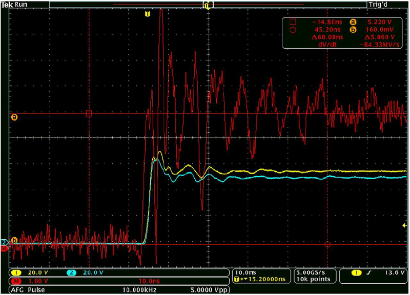
Pseudo differential measurements offer another option for using passive probes and can be adequate for some low frequency measurements. The measurement is performed by making two ground reference measurements and using the scope’s math subtraction between the two scope channels. In Figure 5, the scope subtracted the waveform on CH2 from the waveform on CH1 resulting in the red waveform. Both inputs must be set to the same scale and the probes must be identical and closely matched. Common mode rejection ratio (CMRR) with this technique is poor, as is apparent in Figure 5, particularly at higher frequencies, and can overdrive the scope’s input. CMRR refers to a probe’s ability to reject any signal that is common to both test points in a differential measurement.
Click image to enlarge
Figure 5. Pseudo-differential measurements are limited in performance but adequate for very low frequency measurements with low common mode signals
Differential probes
For most GaN and SiC applications, differential probes are a good choice for accurate low side measurements and some high side measurements. But for higher performance devices, the traditional high voltage differential probe is most likely not the best option due to its inefficient common mode rejection capabilities at higher frequencies. This becomes a significant problem for high side voltage measurements where you need to measure a small differential voltage in the presence of a large common mode voltage during rapid switch node transitions.
A common misconception is that differential probes are floating. In fact, traditional differential probes are based on differential amplifiers which are connected to ground earth. The unfortunate effect is that this connection limits common mode voltage range, causes frequency derating, creates ground loops and limits common mode rejection ratio at bandwidths greater than a few MHz.
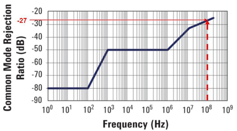
These limitations are especially significant when testing powered GaN or SiC devices with ultra-fast switching rates, and even nominal common mode voltages. For example, a 100 MHz bandwidth differential probe that offers -70 dB CMRR at DC and -50 dB at 1 MHz derates to just -27 dB CMRR at 100 MHz – approximately 22 to one.
Such negative specs can be hard to track down from probe datasheets that don’t promote derating against frequency as a feature. Instead, you’ll need to hunt through the user manual for plots such as that shown in Figure 6. The impact of poor CMRR, however, is easy to calculate. For 600 V of common mode voltage, for example, the resulting error is 27 V (600 divided by 22). This is a showstopper as it simply would not be possible to accurately measure a high frequency 15 V differential signal in the presence of 600 V of common mode voltage using a probe that produces this amount of error.
Click image to enlarge
Figure 6. A 100 MHz bandwidth differential probe derates to -27 dB CMRR as frequency increases
Another consideration for calculating common mode rejection is accounting for the connection between the probe and the DUT. Most common mode rejection specifications only include the probe and do not consider additional connectivity options, such as large hookup clips.
Lacking sufficient probing options, many power designers have resorted to some alternative techniques when it comes to the high side device measurements such as measuring the low side and referring the results to the high side using extensive simulation, examining thermal characteristics, EMI proximity probing, and when all else fails, simple trial and error.
High performance isolated probes
The limitations of single-ended and differentials probes become more pronounced when testing SiC and GaN power devices with very fast switching rates and high nominal common mode voltage. Since the problem of capturing these signals stems from the need for earth ground, it follows that a workable solution would be probe technology that does not depend on earth ground, and therefore would be more or less immune to the effects of high-common mode voltage. Such isolated probes operate entirely through fiber optics and offer a number of advantages including bandwidth up to 1 GHz, large differential voltage range and excellent common mode rejection across all frequencies.
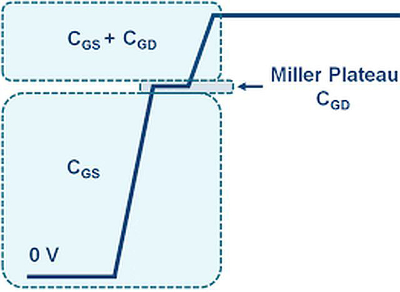
When performing high side VGS measurements, engineers need to see enough waveform detail to confirm simulations and evaluate signal characteristics, such as ringing, compared to the ideal state represented in Figure 7. The high side VGS turns on and the first region depicts the CGS gate source charge time, which is followed by the Miller plateau. Once the channel is in conduction, the gate will charge up to its final value.
Click image to enlarge
Figure 7. This is a representation of the ideal state for high side VGS
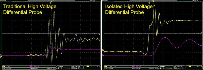
In looking at the comparison of high side VGS measurements using a traditional high voltage differential probe versus a high performance isolated probe shown in Figure 8, it’s clear that it would be very difficult to extract meaningful information and make design decisions based on the measurements provided by the traditional probe.
Click image to enlarge
Figure 8. An isolated high voltage differential probe provides the measurement confidence needed to optimize device performance
In the contrast, the isolated high voltage measurement system offers the resolution and repeatability required to measure and characterize and optimize the performance of such a design. You can clearly see the Miller plateau and the correlation to the switch to node transition. This waveform clearly shows resonance and signal details that were previously hidden, ultimately providing the confidence needed to optimize performance and develop the design without being overly conservative.
High side, low side interaction
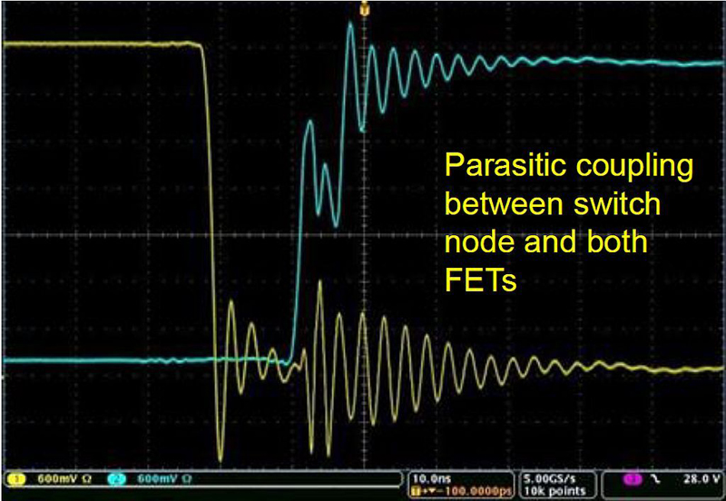
One of the more difficult to diagnose problems, especially for GaN devices that have tight tolerances, is parasitic coupling between the low side switch and the high side gate in the switch node. Figure 9 shows a case where overshoot or ringing from the high side is carrying over to the low side. Such a situation, unknowable without the ability to perform accurate high side measurements, can cause a number of problems ranging from worst case catastrophic failure to simultaneous conduction where both the low side and the high side are turning on at the same time. At a minimum, you'll have switching and efficiency loss and degradation.
Click image to enlarge
Figure 9. The ability to see actual waveforms makes it possible to diagnose and resolve problems such as parasitic coupling between switch nodes
Summary
It certainly no understatement to say that the measurement challenges surrounding half bridges and gate drivers are numerous, but at the same time these challenges must be overcome to take full advantage of the latest wide bandgap materials. This requires proper measurement techniques and capable measurement solutions. Often, issues are not scope driven, but are based on probe selection. High side gate measurements are especially daunting, but many of the challenge involved can be overcome by understanding common mode rejection ratio and how isolated high voltage differential probes can enable accurate, reliable measurement insights even in the presence of high common mode voltage.


