High-Current Designs Utilizing Paralleled MOSFETs in Motor Drive Applications
Selecting the proper MOSFETs by quantifying the effect of their parameters’ mismatch on current distribution
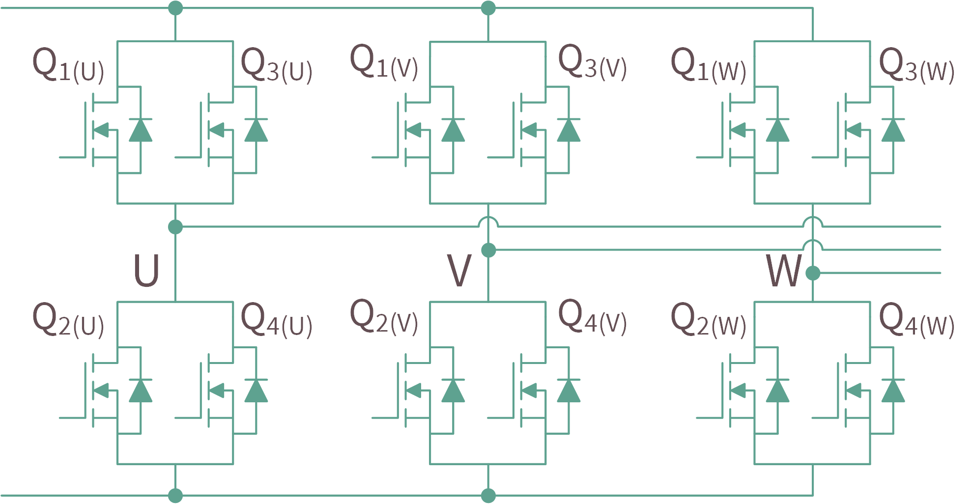
Figure 1. 3-phase inverter with two MOSFETs in parallel per switch
In applications such as motor drives, the half-bridge topology (typically 3 phases) is used to generate an AC power signal that produces a positive or negative torque in an electric motor. High output currents can be achieved only by means of paralleling MOSFETs that form each of the functional switches.
When paralleling MOSFETs, it is necessary to consider the distribution of current among the paralleled devices. Current imbalance, caused by layout asymmetries and unmatched MOSFET parameters, results in imbalanced dissipation distribution between the paralleled MOSFETs.
This article shows the effects of MOSFET parameter mismatch on the current imbalance between paralleled MOSFETs and the resulting average loss imbalance of the corresponding MOSFETs. Specific system properties are considered in order to properly quantify the power losses and the impact on system performance: from layout and switching properties to load current and PWM scheme. Although this kind of analysis is application-specific and strongly individual from system to system, some general conclusions can be drawn.
Additionally, we highlight the relevance of VGS(th) matching between the paralleled MOSFETs and address the effect of transconductance (gfs) on current sharing in combination with the VGS(th) mismatch. While low gfs can improve current balance in paralleling, it is also important to consider the conduction properties since a low gfs could come with higher RDS(on) values.
Evaluating MOSFET power losses with AC output load current
A half-bridge with two MOSFETs connected in parallel at both high- and low-side is used to simulate the effects of MOSFET parameters on the resulting total power losses. The model circuitry, shown in Figure 1, is simplified to the point of being perfectly symmetrical. However, parasitic inductances and resistances of the traces for a representative circuit are still accounted for. MOSFETs Q1 and Q3 represent the paralleled high-side switch.
When analyzing system losses, it is essential to distinguish between instantaneous and average losses. Instantaneous power dissipation is a highly dynamic function. The main contributions to MOSFET losses can be broken down into the following instantaneous losses:
· EON – MOSFET switching loss at turn-on
· EOFF – MOSFET switching loss at turn-off
· PCND – conduction loss of the open MOSFET channel in forward conduction
· PD – conduction loss of the body diode
· EDoff – reverse recovery loss of the body diode
These components are often observed and compared on an individual basis. However, the quantitative contribution of each to the overall losses greatly depends on the nature of the load current and the type of the control scheme being used. Therefore, to compare the relevance of a particular MOSFET parameter to the overall system performance, that parameter’s effect on performance needs to be quantified in a way that is most relevant to the given application.
Average power dissipation in combination with the thermal characteristics determine the temperature of a device and is, therefore, a direct limiting factor for system performance. The average losses can be broken down to show the contribution of switching losses and conduction losses separately:
· PQ1-SW(avg) – average switching losses at MOSFET Q1
· PQ1-CND(avg) – average conduction losses at MOSFET Q1
· PQ1-TOT(avg) – total average losses at MOSFET Q1 (sum of PQ1-CND(avg) and PQ1-SW(avg))
In the relatively simple condition with DC output current, a single PWM cycle is sufficient to provide the information required to estimate the average losses for steady-state operation. Unlike that, calculating the losses for sinewave output currents requires considering at least one whole sine cycle since the current amplitude is different at each PWM cycle.
In this article, the resulting MOSFET losses consider an AC load current as the half-bridge output, being the most relevant in motor drive applications. The output load current is hence a sinewave of a given amplitude, according to the following equation:

The switching modulation scheme applied is SPWM (sinusoidally-weighted pulse width modulation) with the conditions and settings as defined in Table 1. The same SPWM conditions are used in all examples mentioned in this article.
Table 1. Load conditions and SPWM parameters

Click image to enlarge
Power dissipation imbalance and the effect of VGS(th) mismatch
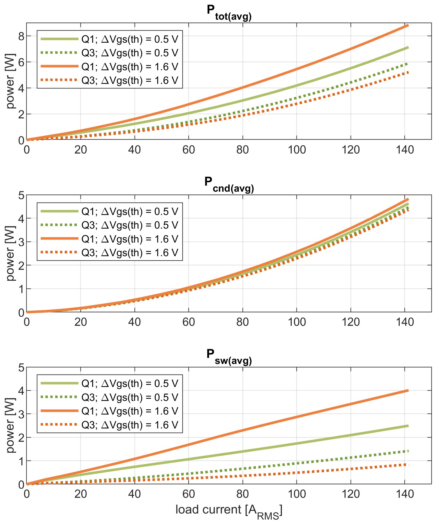
Considering the imbalance associated with paralleled MOSFETs, individual power dissipation is crucial for a reliable system design. Therefore, the result charts in this article show the average power dissipation of an individual MOSFET with relation to the output load current amplitude. Each plot compares the results from at least two different sets of conditions.
The main emphasis in interpreting these results is always given to the power dissipation of that MOSFET dissipating the most power. This MOSFET (i.e., “hottest MOSFET”) acts as the bottleneck for the system output current.
Certain MOSFET parameters, when mismatched, have an impact on current sharing in various ways. The value of RDS(on) has an effect during the conduction of the MOSFETs, while some other parameters (VGS(th), RG, CGS, CGD) influence current sharing during switching. Performing a simulation with a perfect layout symmetry allows the investigation of the effects of individual MOSFET parameters.
Compared to other parameters, the significance of VGS(th) mismatch to the overall performance (dissipation imbalance) comes partially from the MOSFETs’ typical production variation in quantitative terms and mainly due to how they affect the behavior of the imbalance. In a group of paralleled MOSFETs, the one with the lowest VGS(th)will exhibit an increase of switching losses both at turn-on as well as at turn-off, which is not the case for other parameters’ mismatches. In addition, the negative temperature dependency of VGS(th) increases the imbalance even further; however, the temperature dependency is not considered in the following examples.
To highlight the importance of VGS(th) matching between the paralleled MOSFETs, the graphs in Figure 2 compare MOSFET power dissipation using two VGS(th) mismatch examples.
Click image to enlarge
Figure 2. Average power dissipation in MOSFETs Q1 and Q3 (two MOSFETs in parallel)
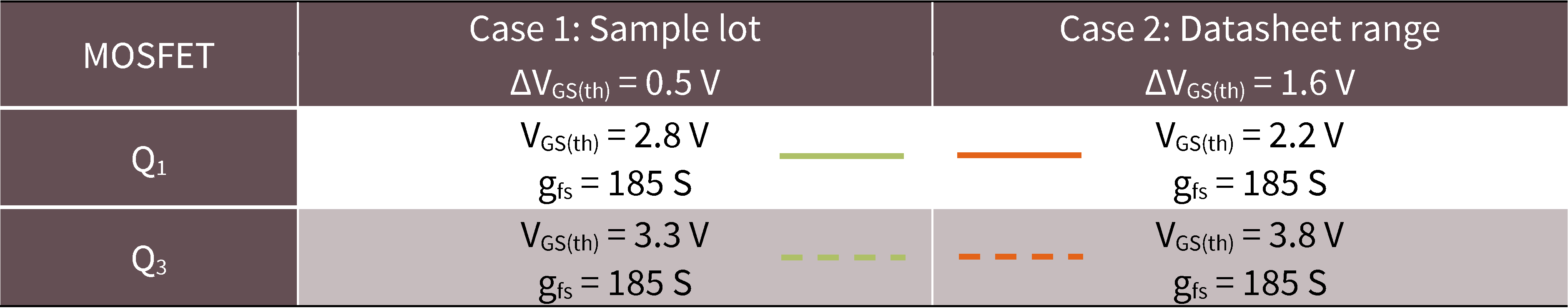
Table 2 shows the combinations of VGS(th) values used in the simulations.
Table 2. MOSFET parameters – VGS(th) mismatch
Click image to enlarge
The orange lines in Figure 2 show the results for what would be the worst-case mismatch of VGS(th) considering the maximum and minimum values according to the datasheet. The power dissipated in Q1 can be double the power dissipation in Q3 for a given output voltage.
Statistically, this extreme mismatch is not very likely; therefore, a more “realistic worst-case” mismatch, considering the parameter spread of a sample lot, is shown in comparison. The green lines in Figure 2 show the results for a smaller VGS(th) mismatch of ∆VGS(th) = 0.5 V.
Power dissipation is proportional to the MOSFET average temperature and thus determines the limit of the system output current since the maximum device temperature must not be exceeded in any individual MOSFET.
Ensuring low current imbalance when paralleling MOSFETs is essential for system size reduction and optimization. Increased current imbalance tends to gravitate the majority of losses towards a single device, diminishing the benefits of paralleling.
Therefore, it is crucial to consider a low production variation of VGS(th) when selecting MOSFETs for paralleling.
Effect of transconductance (gfs) on current sharing
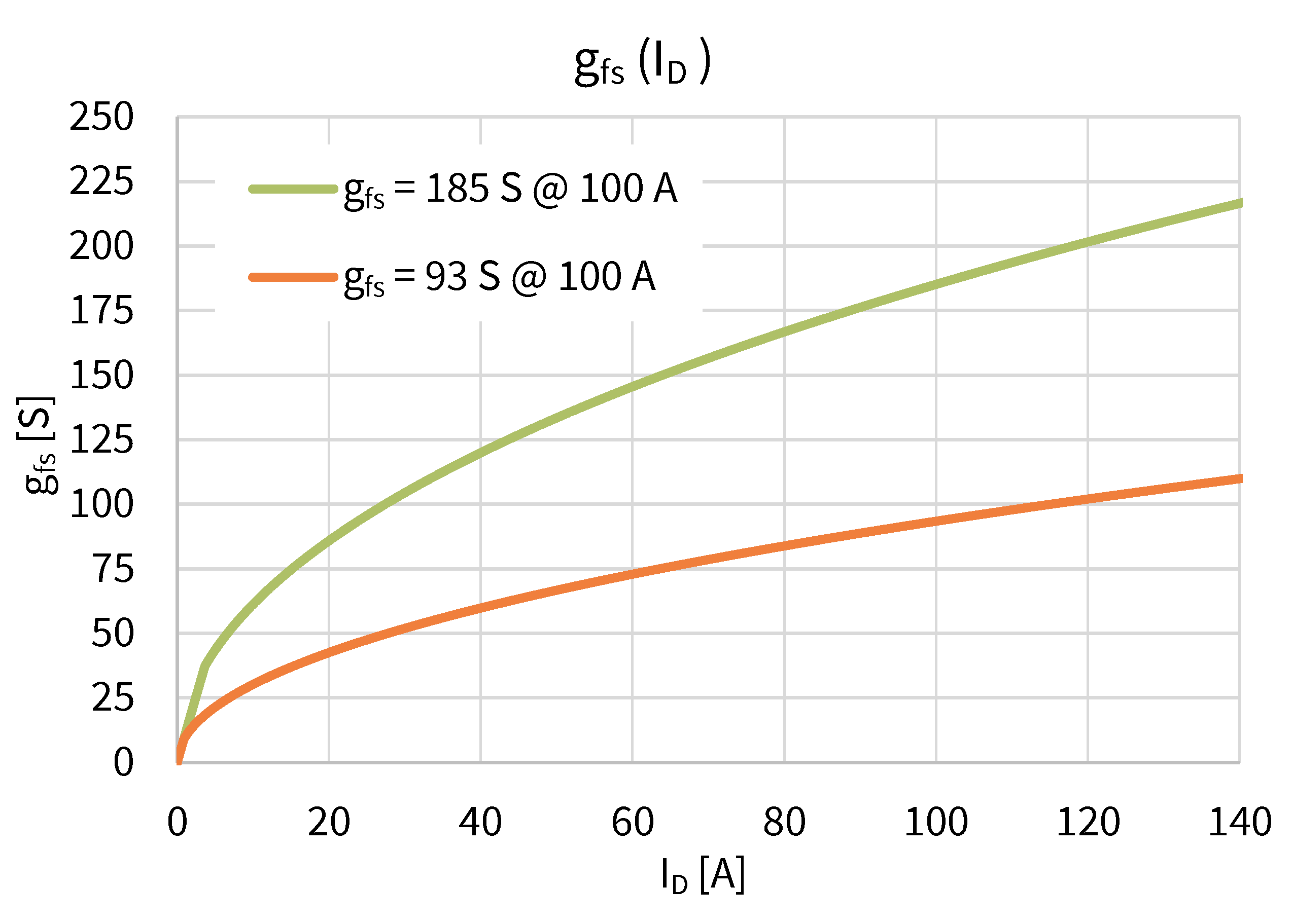
The current imbalance during switching is strongly affected by ∆VGS(th); however, it does not explicitly define the imbalance on its own. An interesting impact on current sharing can be noticed when simultaneously observing the effect of VGS(th) at different values of transconductance (gfs). The gfs value is not constant across the ID range. Figure 3 shows such an example with its full characteristics. The datasheet parameter of gfs (e.g., gfs = 185) is typically a value specified at a given condition of ID, which corresponds to the characteristics as indicated in Figure 3. The full characteristics must be considered in the model in order to carry out an accurate simulation.
Click image to enlarge
Figure 3. Example of gfs vs. ID of OptiMOS technology
The reduction of gfs affects both switching and conduction losses. Since RDS(on) is implicitly linked with gfs, opting for a MOSFET with lower gfs can result in an increase in conduction losses. The lower gfs also slows down the switching, so the switching losses are increased.
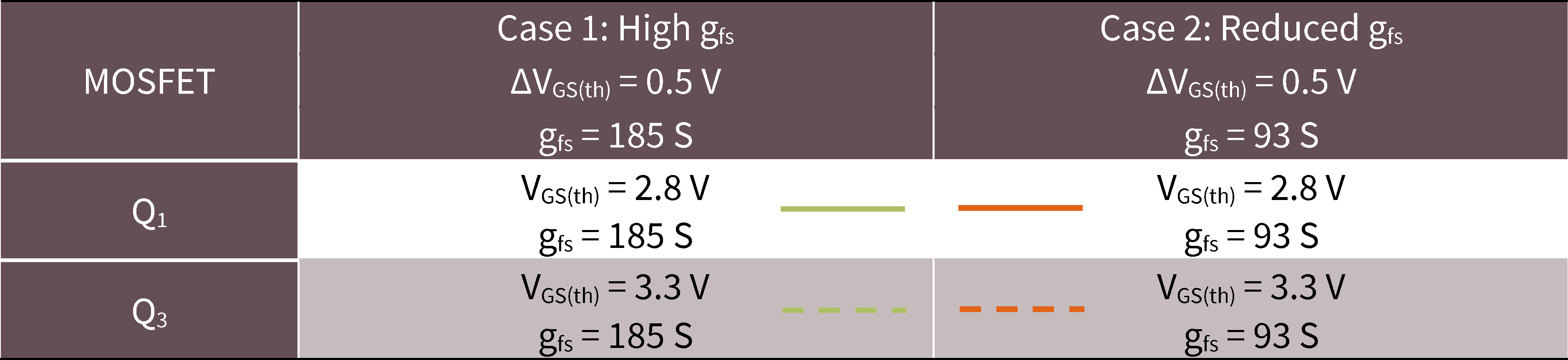
In order to make a fair comparison, in the following example with different gfs values (Table 3), switching speed (diD/dt during switching) is matched via the RG network.
Table 3. MOSFET parameters – gfs reduction @ ∆VGS(th) = 0.5 V
Click image to enlarge
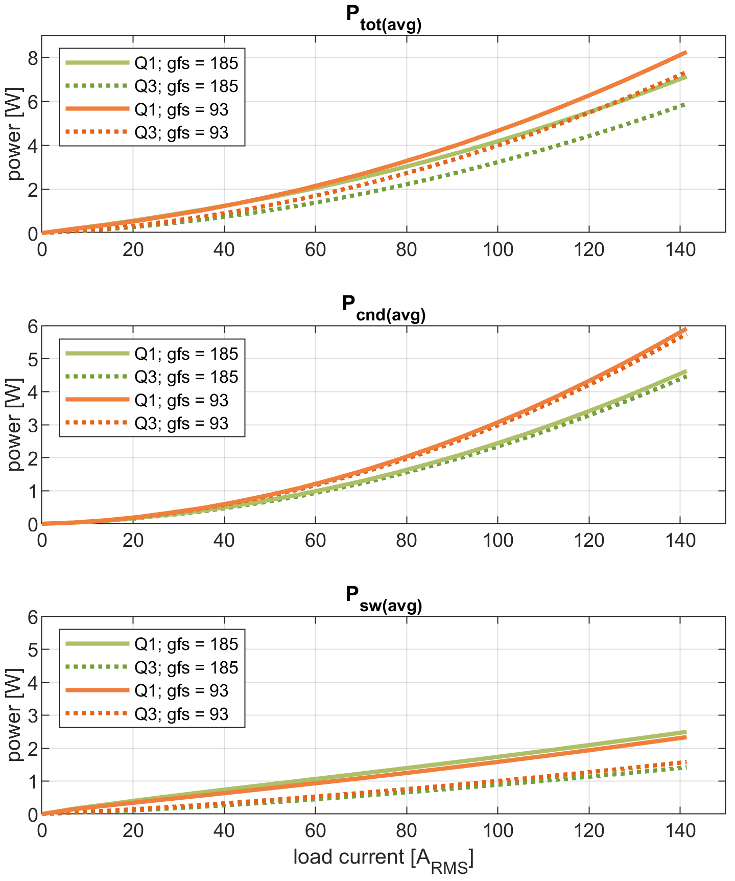
Figure 4. The comparison between the two gfs values, considering the case of VGS(th) mismatch of ∆VGS(th) = 0.5 V between Q1 and Q3. In lower gfs, the Rg value was reduced to match the diD/dt during switching.
Click image to enlarge
Figure 4. Comparison between different gfs values: gfs = 185 S vs. gfs = 93 S @ ∆VGS(th) = 0.5 V (matched diD/dt via Rg)
Reduced gfs at matched switching properties results in an improvement in switching loss imbalance. However, the overall performance is worse since increased conduction loss due to higher RDS(on) increases total loss.
In other words, the increase in conduction losses outweighs the benefits of the improved current sharing.
On the other hand, if switching losses are increased for any reason and become the dominant part of the total loss, the benefit of balancing the switching losses also gains significance. There is a tipping point where improving current sharing justifies the increase in conduction loss.
The bottom line is that the general guidelines can only take us so far – optimization can only be achieved when considering all the system specifics.
Conclusion
In conclusion, the effect of current imbalance on the distribution of power dissipation requires a holistic approach to quantify and interpret the significance of individual parameter contribution.
No matter the cause of the imbalance, the hottest of the paralleled MOSFETs will always determine the limits of system performance, being the system’s “weakest link.” A higher current imbalance leads to a higher loss being accumulated in the single MOSFET.
Therefore, it is evident that improving current sharing will improve system performance simply by reducing the power dissipation in the hottest MOSFET. However, it is vital not to forget the overall power losses when comparing different systems. If balancing the losses results in an overall increase of losses, the outcome may not actually be an improvement.
Additionally, this optimization will differ from application to application, while exact system and control characteristics will also contribute to this outcome. Therefore, it is essential to keep in mind the big picture to determine which device will work best in a given system.
Infineon’s latest generation of power MOSFETs targets applications that utilize paralleled MOSFETs by introducing improvements in current sharing while maintaining low RDS(on) values. Serving the newest and future trends in power converter technologies, Infineon offers a unique product portfolio and supports designers in building highly efficient and cost-effective solutions.
To gain more insights, read the extensive application note “Paralleling power MOSFETs in high current applications” which presents more examples and test results. Alternatively, consider taking the available online training “Balancing paralleled MOSFETs: the importance of parameter spread”.
Additionally, do not miss to check out the available design support documents, reference designs, and simulation models by visiting the related Infineon N-Channel LV/MV Power MOSFET webpage.