With the continuous and fast paced growth of data processing infrastructures, higher power levels that can be delivered in smallest areas are demanded
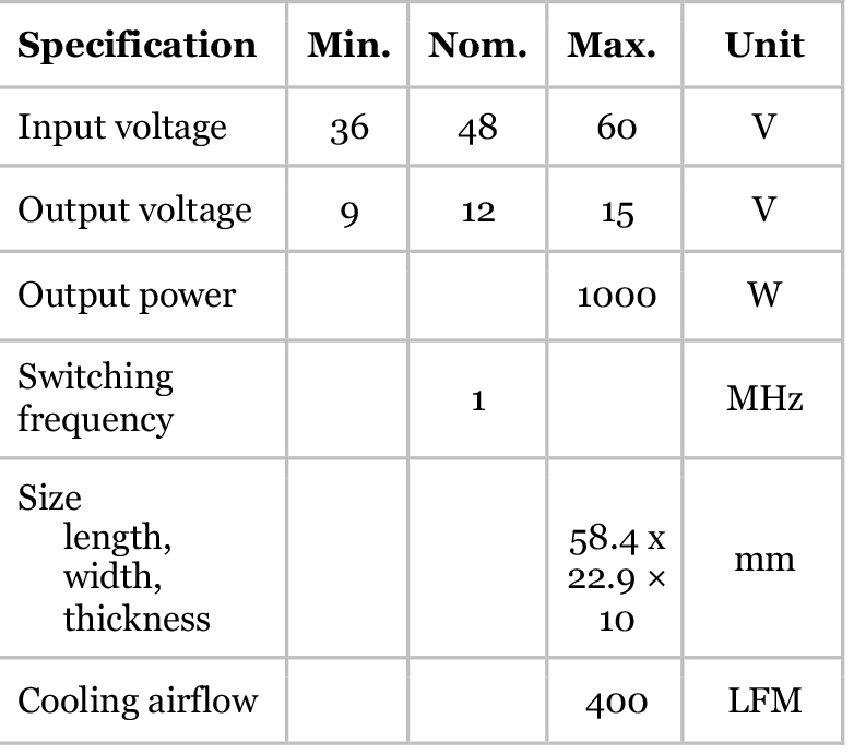
Table 1: Converter specifications
This article addresses the power density demand by presenting a high efficiency, high power density LLC resonant based converter that meets the requirements of modern data center and server rack power delivery systems. This DC-to-DC converter connects the 48 V intermediate bus to a downstream 12 V bus in an unregulated, non-isolated manner and can deliver 1 kW into a 12 V load.
Converter Specifications and Overview
Table 1 shows the key design specifications of the converter.
In addition, the converter module needs to be able to be horizontally or vertically mounted.
Approach Overview
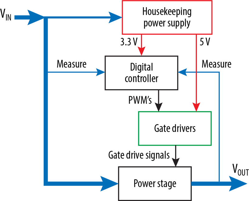
Figure 1 shows the system level block diagram of the converter. A local housekeeping power supply generates the required voltage for the control system. First, the 48 V bus is converted to a 5 V to power the gate drivers followed by the 3.3 V supply that is acquired from the 5 V using a Low Drop-Out (LDO) linear regulator for the microcontroller. Input and output voltages are measured and fed back to the microcontroller to monitor the operation of the unit. High resolution PWM signals are generated by the controller to command the power stage.
Click image to enlarge
Figure 1: Block diagram overview of the module
Topology Selection and Operation Overview
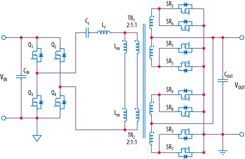
The LLC resonant topology was chosen for this converter and the power schematic is shown in Figure 2. A full bridge primary side configuration generates the pulsed input voltage to the resonant tank circuit. The tank comprises a resonant capacitor in series with the resonant inductor by using the transformer leakage inductance. A high frequency planar transformer with 4:1 turns ratio was designed as a matrix transformer comprising two series 2:1:1 connected sections wound around a single two post core. The transformer magnetizing inductance in conjunction with a pre-determined deadtime setting is used to establish zero voltage switching (ZVS) on the primary side FETs. Switches Q1 & Q4 and Q2 & Q3 are switched at near 50% duty cycle and at 180° out of phase with each other.
Click image to enlarge
Figure 2: Power circuit schematic for the LLC module
Click image to enlarge
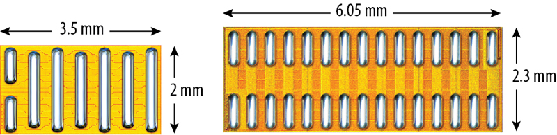
Figure 3: Photo of the bump side of EPC2218 (left) and EPC2024 (right)
Two parallel center-tapped half bridge arms are used in the secondary side together with synchronous rectifier FETs for the output. This synchronous rectification scheme reduces the secondary side conduction losses at high load currents.
Switching Device Selection
The LLC topology is well documented [1-3] and with the advent of new generation eGaN FETs can significantly improve the high efficiency and high-power density capability of this topology. eGaN FETs have figure of merits several times lower than their MOSFET counterparts [4]. eGaN FETs have lower gate charge which reduces gate driver power consumption. The lower on-state resistance (RDS(on)) helps with lowering conduction losses particularly at high load current. The lower output capacitance, (COSS) compared to MOSFETs, enables shorter deadtimes in soft switching applications by reducing the required energy to establish soft switching applications.
The smaller size of eGaN FETs simplifies reducing the size of power converter which increases power density.
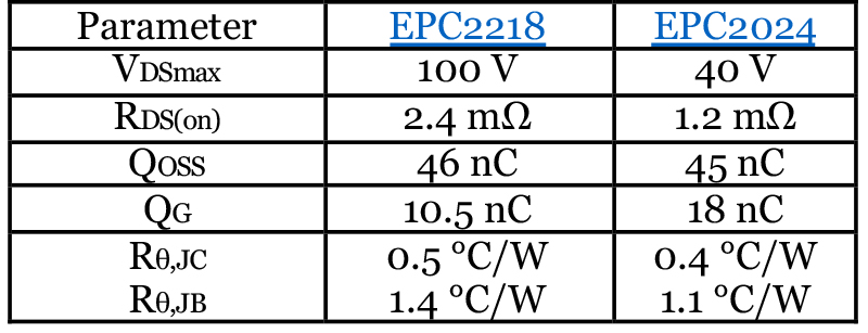
The two eGaN FETs selected for the primary and secondary side of the LLC module are shown in Table 2 and figure 3.
Click image to enlarge
Table 2: Primary (EPC2218) and secondary (EPC2024) side eGaN FET Parameters.
Experimental prototype and Results
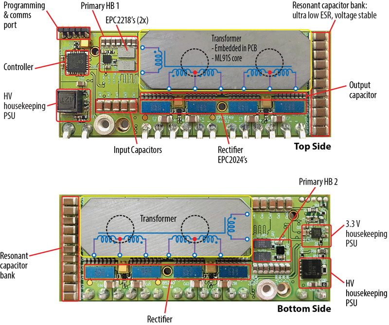
The EPC9149 LLC board top and bottom sides are shown in figure 4 with the various sections highlighted.
Click image to enlarge
Figure 4: LLC board prototype; (a) top side, (b) bottom side
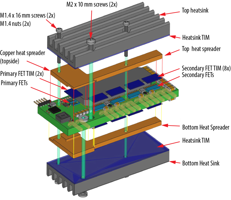
Given that the board is small, a customized heatsink approach is required to meet the allowable operating temperature for the components in the maximum allowable airflow. Figure 5 illustrates the various components of the cooling system and order of assembly for the module.
Click image to enlarge
Figure 5: Thermal solution assembly diagram for the LLC module
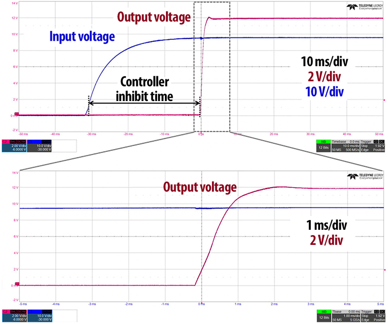
A soft startup process is implemented in the controller to minimize high inrush currents in the tank and minimize voltage stresses across FETs during initial startup and before the output voltage has been established at the nominal operating value. During startup, the microcontroller ramps up the duty cycle in 250 ps steps until it reaches the nominal operating value of around 50%. Figure 6 shows the input and output voltages during startup sequence.
Click image to enlarge
Figure 6: Startup waveform (larger time scale on top and zoomed in version on the bottom)
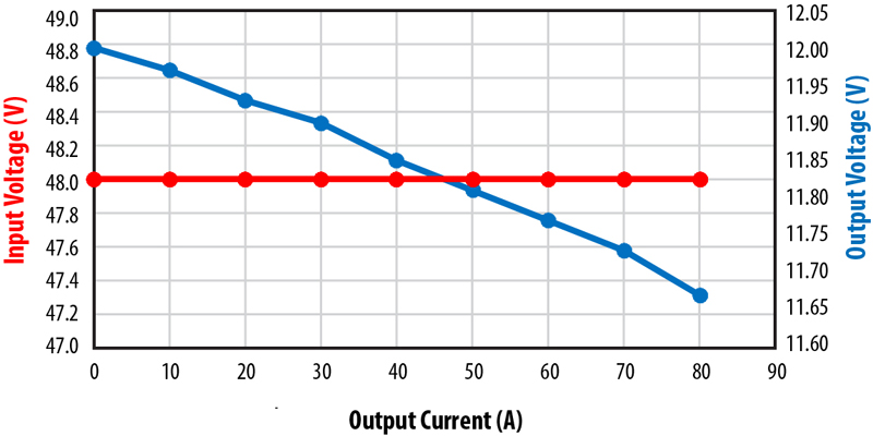
The converter operates in open loop mode as a DC transformer and thus provides no regulation for the output voltage. Operating from a fixed input voltage, as load current increases, the output voltage will drop. The output voltage droop as a function of load current is shown in figure 7.
Click image to enlarge
Figure 7: Output voltage droop vs output current
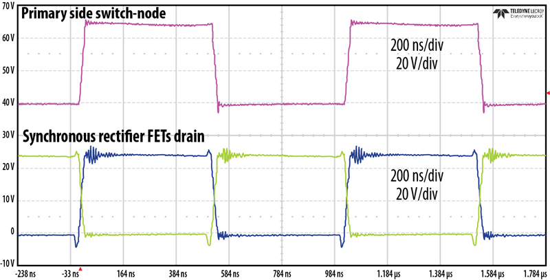
ZVS is achieved in the primary side FETs as can be seen in the waveforms of the switch node in figure 8 due to the absence of overshoot and ringing.
Click image to enlarge
Figure 8: Switching waveforms at 48 V input voltage and 1 kW load, CH2: Primary side switch node (20 V/div) and CH3,4: synchronous rectifier’s Drain voltages (10 V/div)
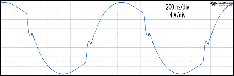
The secondary side synchronous rectifier FETs Drain voltages also experience smooth transitions. The waveforms are captured at full 1kW load power and the resonant circuit tuned to be slightly above resonance. The resonant tank current at this condition is also shown in figure 9.
Click image to enlarge
Figure 9: Resonant tank current at 48 V input, 12 V output voltage, 1 kW full power. (200 ns/div, 4 A/div)
The resonant capacitor is set at 3.96 µF and based on the measured primary current the resonant inductor was found to be 14 nH.
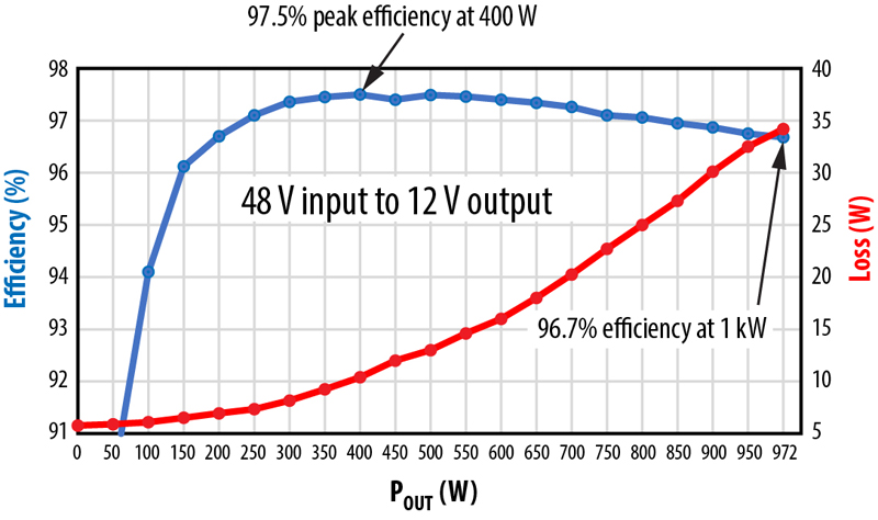
The LLC converter overall efficiency and loss including the housekeeping power supply is depicted in figure 10. The measured peak efficiency is 97.5% and 96.7% full load.
Click image to enlarge
Figure 10: Total efficiency and loss as function of output power at 48 V input voltage and 12 V output voltage
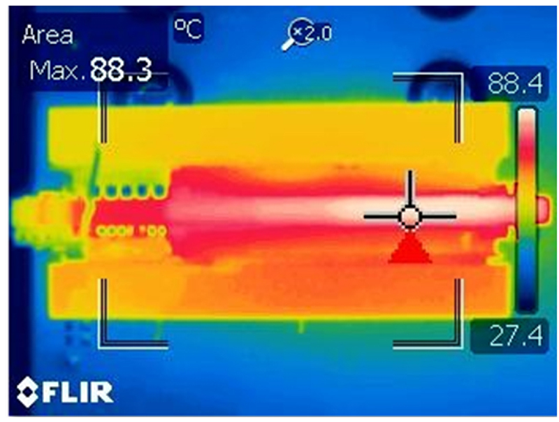
The converter is operated at full load condition with 400LFM forced air cooling and thermal stability was reached in 10 minutes. The temperature of the board and primary side FETs are the hottest areas on the board as shown in figure 11 where the maximum die temperature of 95°C and PCB temperature of 88°C was measured.
Click image to enlarge
Figure 11: Thermal image of the LLC module operating at 48 V input, 12 V output and 1 kW output power
Conclusions
A 1 kW eGaN FET based LLC resonant converter in the ⅛th brick size was presented which achieved 97.5% and 96.7% peak and full load efficiency, respectively and power density of 1227 W/in3.