press x to close
Author:
Joao Pedroso, Technical Product Marketing Manager, KEMET Corp
Date
04/01/2021
 PDF
PDF
Phased arrays work on the principle that the interference between coinciding waveforms with different phase angles can influence the direction of transmission. Using this technique, a two-dimensional array of emitters can steer its aggregated output across a relatively wide angle, perpendicular to the array's surface.
What this means in practice is that radar systems no longer need to rely on a rotating antenna pointing directly in the direction of interest. These systems, known as active electronically steered arrays, or AESA, are now widely used in airborne, sea and land systems by the military, as well as in some civilian applications.
Because they require an array of multiple, small transmitters, as opposed to a single, powerful transmitter, they do carry a higher cost. However, the benefits, as outlined below, can outweigh this additional cost, particularly in high-reliability applications. Part of the cost comes from replicating the transmitters, but the way each transmitter is designed also has an impact. Typically, an AESA uses at least one Gallium Nitride (GaN) transistor in each transmitter, as they offer significant advantages. This design choice has wider consequences, however, which are discussed in this article.
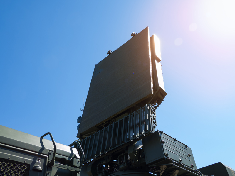
Modern radar design
Not surprisingly, radar systems are one of the main applications for AESA technology. As there is no need to physically move the antenna, there are no (or, at least, fewer) moving parts involved. Having fewer potential points of failure supports their use in military applications, where the harsh environments involved can be particularly punishing on sensitive electric motors. In addition, because the antenna is based on an array that can easily feature over 1,000 transmitters, if one transmitter fails the antenna can continue to function with hardly any deterioration in performance. The same is not true for a conventional antenna with only one transmitter. The nature of the antenna's emissions also makes it more difficult to detect the array using counter-surveillance equipment. For the same reason, it is less susceptible to jamming techniques.
However, having such a large array of transmitters, each of which needs its own supporting electronic subsystem including an amplifier and power supply, does present its own challenges. Space can easily become an issue, which is one reason why AESA systems now employ power transistors based on wide bandgap (WBG) materials. Most notably, Gallium Nitride, or GaN power transistors. GaN technology brings a level of efficiency that supports the frequency and power output levels used in AESA systems, as outlined in Table 1, below.
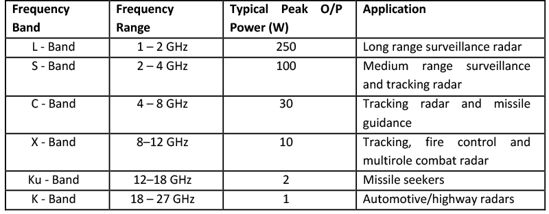
Click image to enlarge
Table 1: AESA systems can support a wide range of frequencies and power output levels for specific use-cases
Power transistors based on WBG technology, such as GaN, are able to operate at higher power levels and higher frequencies, more efficiently than silicon-based power MOSFETs. As such, they are gaining adoption in a wide range of applications where these attributes are important, including AESA, electric vehicle inverters and onboard chargers, and solar inverters.
It is the nature of WBG substrates that makes them so suitable to high-power applications. When measured against silicon, they exhibit a higher breakdown voltage and greater electron mobility. These features also mean they have better thermal conductivity than silicon substrates; the thermal conductivity of GaN is around 15% better than silicon. Furthermore, the low thermal expansion of their lattice structure means that power transistors based on GaN have much better thermal efficiency, allowing them run cooler than silicon and operate at higher temperatures. This ultimately results in higher power density, supporting their use in arrays. In long-range surveillance applications (see Table 1), the output power of each transistor can easily reach 200 W, so high efficiency, high power density and good thermal conductivity are priority requirements.
The impact of GaN on system design
As mentioned earlier, using GaN power transistors has a systemic impact. It puts greater demand on all of the components, not least the passive components. The high voltage levels and frequencies involved will influence the construction of the capacitors used. As the industry leader in polymer capacitors, KEMET has used all its knowledge in the development of capacitors for AESA applications.
For example, the system requirements outlined make the use of conventional options unadvisable at best. This includes wet tantalum and ceramic capacitors, but the specific demands of high-reliability applications can also exclude the use of other conventional solutions, such as tantalums with a solid manganese dioxide (MnO2) electrolyte. This is partly due to the possibility of combustion in the event of failure.
Thanks to its position as the preeminent tantalum technology manufacturer, KEMET has made significant advancements in the materials used to manufacture polymer capacitors. Until recently, capacitors based on dielectrics formed from tantalum pentoxide (Ta2O5) would be restricted to low voltage applications. Today, KEMET can supply polymer tantalum capacitors with properties that are well matched to the performance offered by GaN transistors. The properties engineers focus on here include the equivalent series resistance (ESR); by keeping the ESR as low as possible, heat dissipation in the device is minimized. Another important figure of merit is voltage tolerance; KEMET capacitors feature a tolerance of above 60 V, rather than the 28 V more commonly associated with these capacitors. The ability to operate at switching frequencies in the region of 600 kHz is also important, as this is commensurate with the switching frequencies of GaN transistors. And as with all components today, a smaller form factor is better.
In addition to these performance gains, KEMET's tantalum capacitors have a 'fail safely' characteristic, making them safer in high-reliability applications. The low ESR also supports fast context switching, enabling them to respond quickly to system changes such as pulsed signals. KEMET has been able to make these advancements thanks to its expertise in materials science. The capacitors it produces have a mean time between failure (MTBF) that is an order of magnitude better than other tantalums available. In addition, they are less prone to degradation over time, meaning they support the long time-in-service associated with military and aerospace applications.
Another benefit of the polymer tantalums produced by KEMET is their operating voltage, which does not need to be derated in the way standard tantalums must. With operating voltages of 63 V, they can support the applications associated with GaN technology. Figure 1, below, provides an exploded view of the T540/T541 Series from KEMET which is suitable for AESA applications.
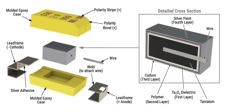
Click image to enlarge
Figure 1: The T540/T541 tantalum capacitor developed and manufactured by KEMET
Conclusion
The features offered by AESA make this technology viable in a wide range of applications. As well as its used in military radar, many vehicles are becoming more reliant on obstacle detection and avoidance; radar and lidar are among the technologies being explored here. Similarly, automated robotic devices need range finding and obstacle detection solutions that are reliable and unobtrusive. These are just some examples of emerging applications where AESA could be deployed in the near future.
With the continued commercialisation of WBG technologies such as GaN and silicon carbide (SiC), their use is set to increase. This will create a need for passives that are better suited to operate with these high-performance devices. With a vast amount of experience and expertise in the development of advanced capacitors, KEMET will continue to meet this need.