Design considerations for resonant converters
Figure 1: Resonant driver for high-power LED-lighting applications.
Solid-state lighting applications such as streetlights and industrial lighting demand drivers that offer better efficiency than the traditional flyback topology in the 50—250 W power range. As LED-emitter performance continues to improve, solid-state lighting is able to offer advantages such as lower energy consumption and longer lifetime in applications that metal-halide or sodium-type lamps traditionally address. These include street lighting and high-bay lights or spotlights in locations such as car parks, toll plazas, fuel stations, warehouses, and factories. The performance advantages LEDs offer enable enterprises to reduce operating costs and improve green credentials, and can help authorities reduce utility bills and maintenance overheads. Growth markets such as these require drivers that offer high efficiency at higher power levels than those of typical domestic retrofits or interior luminaires. These lower-power applications have typically relied on the basic flyback-converter topology, which is relatively simple and is often a good choice for isolated LED drivers below 50 W. In the 50 W to 250 W power range typical of streetlights and high-bay lights, however, the flyback becomes bulky and less efficient compared to a topology such as the resonant converter. The resonant-converter topology offers several benefits at high power levels, including electrical isolation, high efficiency, small magnetic components, and no need for electrolytic capacitors at the output. These advantages enable engineers to achieve high power density. A resonant LED driver follows the same basic design as a resonant power supply. It consists of a two-stage system with a front-end PFC (power-factor-correction) stage followed by a resonant isolation and step-down stage with a rectifier and filter at the output. The key difference between the two designs lies in the control system: The power supply produces a regulated constant output voltage, whereas the LED driver must produce a constant output current. Resonant-LED-driver operation Figure 1 shows the basic schematic of an LED driver using a resonant topology. The front-end PFC stage consists of a boost regulator that converts the full-wave rectified AC line voltage to a DC bus voltage usually between 400 V and 500 V. The DC bus voltage feedback loop responds slowly over many AC line cycles so that the MOSFET on time remains essentially constant during a cycle. Control ICs often increase the on time as the AC line cycle approaches a zero crossing. This serves to compensate for crossover distortion and reduces THD (total harmonic distortion). The majority of controllers operate in CrM (critical conduction mode) at the boundary between continuous and discontinuous conduction modes. The off time varies during the AC line cycle producing an approximately sinusoidal AC input current in phase with the voltage. The converter designer must choose the PFC inductor's value to avoid saturation at IPK—the peak current—and maximum operating temperature.
The back-end stage consists of an LLC resonant converter that converts the DC bus voltage to a DC output of lower voltage and constant current. The transformer is the core element providing isolation and voltage conversion. In figure 1, the transformer exhibits a high primary-leakage inductance that forms a resonant circuit with the series capacitor, which also provides DC blocking. An alternative approach is to use a standard transformer design and add an external resonant inductor. In the basic LLC resonant-converter section, the transformer-secondary circuit consists of two windings and two rectifier diodes (Figure 2). These are normally Schottky diodes to minimize conduction losses, although high-current designs may use MOSFETs as synchronous rectifiers. Most of the ripple at the output is at twice the switching frequency, which allows the stage to use ceramic filter capacitors in conjunction with an inductor to ensure sufficiently low ripple at the output. The half-bridge switches operate at 50% duty cycle and the controller regulates the output voltage by varying the switching frequency. The controller can also effectively regulate the LED driving current by adjusting the frequency. Hence, the designer can select the frequency to provide the necessary drive current for any number of LEDs that connect to the output up to the maximum 60-V low-voltage safety limit. The half-bridge resonant stage has two resonant frequencies. The series inductor, Lr, and resonant capacitor, Cr, determine the first. Cr and the transformer's magnetizing inductance, Lm, determine the second. Soft switching will occur while the frequency remains in the inductive region.
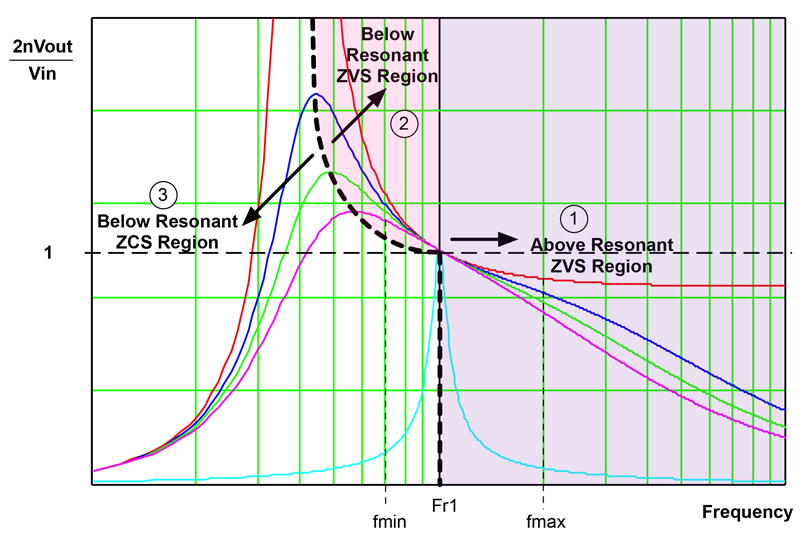
Circuit and transformer design You can model the LLC resonant circuit relatively easily, and then simulate the model in order to analyze the converter's frequency response. Divide the characteristics into three regions based on the three different modes of operation (Figure 3). A key task in designing the resonant circuit is to optimize the ratio between the transformer's magnetizing inductance, Lm, and the resonant inductance, Lr, to control the gain curve's steepness while minimizing circulating power losses. Aim for ratios between 3:1 and 10:1. You can determine Lr and Cr values by running several simulations or calculate them from the maximum Q value and your target resonant frequency. Calculate the maximum Q that allows the converter to stay in ZVS (zero-voltage switching). The maximum Q occurs at the minimum input voltage and the maximum load. Simple methods for calculating the necessary values make use of a spreadsheet or Mathcad script. Several transformer-design methods exist. The most complex challenge lies in incorporating the Lr. Often the engineer will measure a sample transformer's Lr, plug that value back into the simulation, and recalculate the circuit parameters based on the transformer's characteristics.
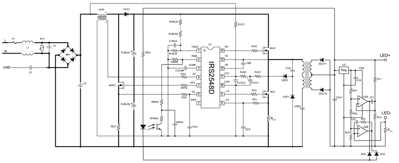
Controlling the resonant driver The resonant converter requires a control IC. Using a combination PFC-plus-half-bridge driver IC, such as the IRS2548D for example, can help to reduce the driver's component count and size. These ICs provide all the functionality necessary for controlling the front-end PFC circuit and the resonant half bridge including a floating high-side gate driver for the upper bridge MOSFET. The controller can adjust the half-bridge frequency using a conventional feedback circuit and opto isolator. It senses the output current through a shunt resistor and compares that measurement to a reference using an op-amp located on the secondary side. The error signal drives the opto diode and the transistor sinks current from the IRS2548D frequency control input to increase the frequency, which reduces the output current to the target level. Adding a voltage-sensing circuit can prevent the output voltage from exceeding a set level in the event of an open-circuit failure. There are several ICs available for such applications that integrate both voltage and current feedback op-amps with an accurate reference and combine the amplifier outputs to drive a single opto isolator. A complete driver using the IRS2548D controller requires a small number of external components (Figure 4). Optimizing the PFC-inductor and transformer selection helps minimize the driver's size. www.irf.com
 Single.jpeg)