
The CIBH diode concept
Figure 1: Application range of high power modules. A different optimization of devices is required, indicated by the attributes "soft" and "fast"
A new technology for the vertical architecture of free wheeling diodes is introduced, which is optimized for applications with high switching frequencies. To minimize the turn off losses of the diode and the turn on losses of the IGBT, a diode with the CIBH (Controlled Injection of Backside Holes) concept is implemented. The CIBH allows to reduce the charge stored in the diode by minimizing the wafer thickness and reducing the doping concentration of the backside emitter, whereas an excellent switching softness remains even under extreme switching conditions. The advantage of the CIBH technology for high power applications is shown by investigations in high voltage modules with 1500A current rating and comparisons to state-of-the-art FWDs. The field of applications for 3300V modules becomes wider. Infineon Technologies has recently introduced a new module which was designed for the needs of applications with moderate switching frequencies and very high stray inductances. But there are also inverter concepts which require higher switching frequencies at moderate values of stray inductances (Figure 1). For the latter applications the focus of the chip development has to be on the reduction of the switching losses. Special attention was paid to the diode. The stored charge carriers not only determine the turn off losses of the diode but also influence the turn on losses of the IGBT. The charge in the diode can be reduced by decreasing the device thickness, lowering the backside emitter efficiency and reducing the carrier lifetime. The first two mentioned measures lead to a worsening of the softness of the switching behavior of the diode. To minimize the switching losses of a module, a concept for the diode is desired, which allows a reduction of the device thickness and the backside emitter efficiency by a large extent, but still provides a good switching softness. The CIBH diode is a concept, which improves the switching softness of the diode under extreme switching conditions like high DC link voltage, low current and high stray inductance, but does not have a negative influence on the trade off between on state losses and switching losses at moderate switching conditions.

The CIBH Concept The performance improvement of the CIBH diode is achieved by implanting buried p doped layers at the cathode side in front of the n+ cathode. During reverse recovery the buried p-doped areas inject holes in the base region improving the ruggedness and softness of fast diodes. Figure 3 shows the cross section of the electric field between the p-doped areas along the dashed line shown in Figure 2 and compares the electric field distribution of the reference and the CIBH diode at the same time during reverse recovery. The reference diode is a state-of-the-art emitter controlled diode with the same thickness. The figure shows that the CIBH diode circumvents the evolution of a high electric field peak at the cathode side effectively by the fore mentioned injection of holes. Plasma providing free charge carriers remains longer at the cathode side due to these injected holes. The plasma removal out of the base region is therefore slowed down and leads to soft reverse recovery. At the time when the whole plasma is completely extracted out of the base region and the electric field reaches through to the highly p doped areas, the injection of holes increases drastically and no snap-off can occur up to very high DC link voltages which are applied to the diode. Furthermore a critical Egawa like field distribution, which means that high electric field strength occurs both at the anode and cathode side, will be suppressed by the hole injection compared to the reference diode without p doped areas (Figure 4). Therefore positive feedback of anode and cathode side carrier generation is avoided, which otherwise might results in destruction of the diode. This is the reason for the improved bulk ruggedness which is hindering destructive mechanisms like current filamentation.

Measurements A high voltage module with 24 diodes in parallel and a rated current of 1500A is investigated. In this large module the advantages of the CIBH concept become obvious. Figure 5 shows a CIBH diode recovery under extreme switching conditions. High values of stray inductance (LS = 320nH) and DC link voltage (VCE = 2300V) combined with low temperature (T = 25°C) and low current (ICE = 300A) lead to a massive current snap off and oscillations at a state-of-the-art fast diode optimized for low switching losses. In contrast the paralleled CIBH diodes show a very soft switching behavior without snap-off even at a high DC link voltage and with a stray inductance well above the required level. Additional charge carriers which are provided by the hole injection from the structured p-doped areas in the backside of the device can be seen in the recovery current waveform of Figure 5. This effect we called Dynamic Self Damping Mode. In a self adjusting way this effect suppresses oscillations and provides enough charge carriers to avoid effectively snap off under extreme switching conditions. So the current cut off - self protection allows to design in this diode into applications with high stray inductances.
The advantages of the thin CIBH diode can be clearly seen in Figure 6, which shows a direct comparison to a soft reference diode with high reverse recovery losses. The fast CIBH diode provides the same soft switching behavior as the soft reference diode.
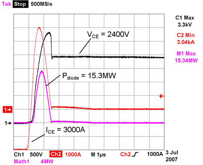
In inverters with higher stray inductances it is possible to reduce the diode switching losses by 25% with the same on state losses. This leads consequently to reduced IGBT turn on losses at the same time. Figure 7 shows a diode recovery which is done under severe test conditions far above the real application conditions. Peak power values above 15.3MW for a FZ1500R33HE3 module have been reached without destruction. The test conditions are VCE=2400V, ICE=2*Inom=3000A and a module temperature of Tj=150°C. The results guarantee a large safety margin to the data sheet peak power values. Conclusion A module with a CIBH diode has been successfully introduced. This diode concept leads to a great reduction of the diode turn off losses and the IGBT turn on losses, but still offers a very soft switching behavior even under extreme switching conditions due to the Dynamic Self Damping Mode. The new diode concept is a breakthrough for FWDs in modern high power / high voltage inverters. In combination with the Infineon trench cell and field stop technology a new benchmark is set in both softness and minimal total losses for high power IGBT modules. www.infineon.com


