Author:
Bilge Bayrakci, Analog Devices, Inc.
Date
11/02/2020
 PDF
PDF
Click image to enlarge
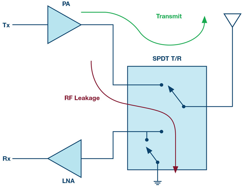
Figure 1. Antenna switch.
Multiple input, multiple output (MIMO) transceiver architectures are widely used in the design of high power RF wireless communications systems. As a step into the 5G era, massive MIMO systems covering cellular bands are now being deployed in urban areas to meet the emerging demand for high data throughput and a new variety of services. The availability of highly integrated single-chip baseband transceiver solutions, such as ADI’s new ADRV9008/ADRV9009 family of products, made this achievement possible. Similar integration toward lower power consumption for thermal management and smaller size for cost is still needed at the RF front-end section of these systems in order to accommodate more MIMO channels.
MIMO architectures allow the RF power requirements on building blocks, such as amplifiers and switches, to be relaxed. However, as the number of parallel transceiver channels increase, the complexity of the peripheral circuits and power consumption scales accordingly. ADI’s new high power switches in silicon technology are designed to simplify the RF front-end designs by eliminating the need for peripheral circuits and reducing power consumption to negligible levels. ADI’s new high-power switches in silicon offer RF designers and system architects the flexibility to increase their system complexity without RF front ends becoming a bottleneck in their designs.
In time division duplex (TDD) systems, there is a switch function incorporated at the antenna interface to isolate and protect the receiver input from transmitted signal power. This switch function can either be used directly at the antenna interface in relatively lower power systems, as shown in Figure 1, or used on the receive path, as shown in Figure 2, for higher power applications to ensure proper termination to the duplexer. Having a shunt arm on the switch outputs will help to improve the isolation.

Click image to enlarge
Figure 2. LNA protection switch.
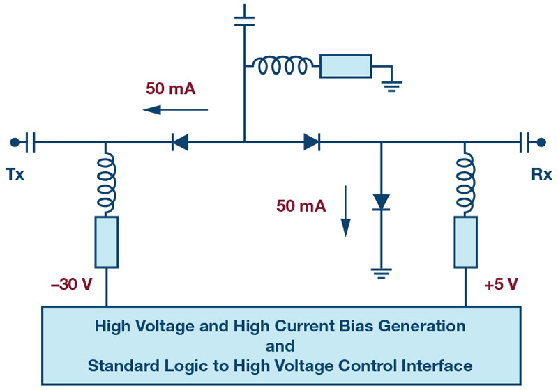
PIN diode-based switches have been the preferred solutions due to their low insertion loss characteristics and high power handling capabilities. However, their need for high bias voltages to reverse bias for isolation and their need for high current to forward bias for low insertion loss are the shortcomings in the design of massive MIMO systems. In Figure 3, a typical application circuit is shown for a PIN diode-based switch and its peripherals. Three discrete PIN diodes are biased through their bias-tee circuits and are controlled through a high-voltage interface circuit.
Click image to enlarge
Figure 3. PIN diode switch.
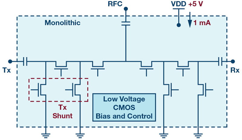
ADI’s new high-power silicon switches are better suited to massive MIMO designs. They run on single 5 V supply with less than 1 mA bias current and do not need external components or interface circuits. In Figure 4, internal circuit architecture is shown. A FET-based circuit operates on low bias currents and low supply voltages, bringing down the power consumption to negligible levels and helping the thermal management at the system level. Besides the ease of use, the device architecture yields better isolation as more shunt arms are incorporated on the RF signal paths.
Click image to enlarge
Figure 4. ADRV9008/ADRV9009 Silicon switch.
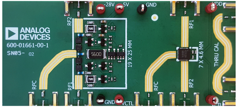
Figure 5 shows a side-by-side comparison of printed circuit board (PCB) artwork between PIN diode-based switch and new silicon switch on a single-layer PCB design. The silicon switch can fit into more than 10× smaller PCB area. It has simplified power supply requirements and does not need high power resistors.
Click image to enlarge
Figure 5. Side-by-side comparison of a PIN diode-based switch design to a silicon switch.
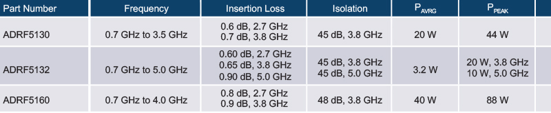
ADI’s high power silicon switches can handle an RF peak power of up to 80 W—that is enough to cover, with margin, the peak-to-average power ratio requirements for massive MIMO systems. Table 1 shows ADI’s family of high power silicon switches that are optimized for different power levels and various package options. These devices inherit the intrinsic advantages of silicon technology and yield better ESD robustness and part-to-part variation compared to its alternative solutions.
Table 1. ADI’s New High Power Silicon Switch Family
Click image to enlarge
Massive MIMO systems will continue to evolve and there will be further need for even higher levels of integration. ADI’s new high power silicon switch technology is well suited for multichip module (MCM) designs to integrate with LNAs to offer a complete, single-chip solution for TDD receiver front ends. ADI will also scale new designs toward higher frequencies and will lead similar solutions for millimeter wave 5G systems. Circuit designers and system architects will also benefit from the advantages of ADI’s new silicon switches in other applications, such as phased array systems, as ADI expands its product portfolio with high power silicon switches toward X-band frequencies and higher commonly used frequency bands.


.jpg)