High-speed isolation in ultra-low-power applications
Several applications can benefit from a new class of devices
Isolation has been considered a necessary burden by designers. It is necessary because it makes electronics safe for anyone to use. It is a burden because it limits communication speed and consumes a lot of power and board space. Old-technology optocouplers and even many, newer digital isolators consume so much power that certain types of applications have not been practical. In this article we will examine the latest developments in ultra low power isolation, how it relates to the available technologies, and how it has been achieved. We will also explore several applications that can benefit from this new class of devices.
The advent of the modern optocoupler about 45 years ago was a great step forward for designers. They allowed feedback in power supply control circuits, signal isolation in communications to break ground loops and communications to high side power transistors or current monitors. In the 1970’s there was a proliferation of optoelectronic devices. These shaped the development of communications standards such as RS232, RS485 and industrial busses like 4-20mA current loops and DeviceNet and Profibus.
The capabilities of the optical isolation shaped many of the properties for these communications busses due to the limits of the isolation devices. Over the next twenty years, the changes in isolation technology were largely incremental until 2000 when the first of the new chip scale digital isolators were introduced. These new devices were based on inductive coupling through chip scale transformers, GMR materials and later through differential capacitive coupling.
The new technologies were capable of vastly higher speeds and substantially lower power levels than the older optocouplers, but the standards were in place and many of the capabilities of the new devices such as high speeds have not been fully utilized since the existing standard interfaces did not require it.
Digital Isolation
Digital isolators’ use of standard packaging and IC processes to build their encoding and decoding electronics makes adding digital functionality straightforward. Low power consumption, support for low supply voltages and high levels of integration have become the primary design advantages of the non-optical isolators. Innovation that moves isolation into much higher speeds or much lower power will allow support of the most demanding new interface standards. Currently the power consumption in digital isolators while significantly lower than the optocoupler needs to be two to three orders of magnitude lower to allow entry into new application spaces. High performance isolation has not been able to achieve this goal until now.
Comparing Technologies
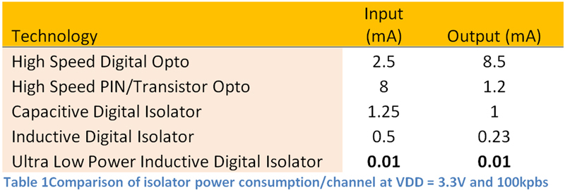
The driver of performance in isolation devices is a combination of the data-encoding scheme and the efficiency of the medium used to transfer the data. For this discussion we will focus on the aspects that determine power consumption. The encoding and decoding schemes can broadly be divided into Edge encoding Pulse based systems and level encoded systems. At its simplest, a level-based system must constantly push energy across the isolation barrier to hold a dominant output state, while sending no energy across the barrier to represent the recessive output state.
In an optocoupler, the energy transfer is mediated by light, which has poor efficiency when compared to creating electric or magnetic fields directly, and poor detection efficiency at the receiving element. So simple transistor or PIN diode based optocouplers have to expend a lot of energy creating light to hold the output in the on state, but the receiver expends little energy to receive the signal. This can be seen in Table 1 with the power consumption of the PIN diode receiver optocoupler. On average high input current and low output current characterize this type of optocoupler.
Click image to enlarge
Faster digital optocouplers have reduced the amount of light required to maintain a state by adding active amplification to the receiver. This reduced the average current required for the LED, but the receivers have relatively large quiescent current so the power consumption has not really diminished it has been pushed to the receiver. Lowering the required power would require raising the efficiency of the LED and receiver element, or changing the encoding scheme. This has been why the advances in optocoupler technology have been incremental for so long.
Capacitively coupled digital isolators
In many capacitively coupled digital isolators, the system is actually similar to the optocoupler. This type of device uses a high frequency oscillator to send a signal across a pair of differential capacitors. The oscillator much like the LED of an optocoupler consumes power to send the active state and turns off to send the recessive state. The receiver has active amplifiers that consume bias current for either state. As shown in Table 1 due to the high coupling efficiency of the capacitors, the overall current consumption is significantly better than the optocoupler options.
It should be noted that the power level in the digital isolator would be about the same if it used inductive coupling instead of capacitive. In this case it is primarily the encoding scheme that sets the minimum power level, especially at low data rates.
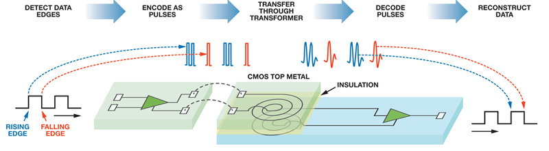
The iCoupler-based digital isolators from Analog Devices such as the ADuM140x series utilize a second encoding scheme, as shown in Figure 1. In this scheme edges are detected at the input and encoded as pulses. In the case of the ADuM140x one pulse represents at falling edge, and two pulses represent a rising edge. These pulses are coupled to the secondary through small on chip pulse transformers. The receiver counts pulses and reconstructs the data stream. The pulses themselves are robust to get good signal to noise ratio, but only 1nS wide so the energy per pulse is low. This has the very nice property that when no data is changing, the state is held at the output in a latch and almost no power is consumed. This means that the power consumption is simply the integrated energy delivered in the pulse stream plus some bias currents. As the data rate goes down the power goes down linearly all the way to DC. Again it is the encoding scheme that delivers the reduction in power consumption rather than the specific medium of data transfer, this scheme could be implemented in capacitive or even optical systems.
Click image to enlarge
The pulse-encoding scheme is not a low-power panacea. Its drawback is that if there are no logic changes at the input, then no data is sent to the output. This means that if there is a DC level difference due to the start up sequence that the input and output would not match. The ADuM140x addresses this condition by implementing a refresh watchdog timer on the input channel that resends the DC state if no activity has been detected for more than 1μS. The result of this design is that this encoding scheme no longer continues to reduce power consumption once the data rate is below 1Mbps. The part is effectively always running at least 1Mbps so the power consumption does not continue to fall for low data rates. Even so, the pulse encoding scheme provides lower average power when compared to the Level sensitive schemes as shown in Table 1.
Pushing the low power envelope
The ADuM140x pulse-encoding scheme was originally optimized for high data rates, not absolute lowest power consumption. This encoding scheme has considerable potential for further power reduction especially in the DC to 1Mbps frequency range. This data range is where the bulk of the isolation applications are found, especially the ones that require low power.
The following innovations were implemented in the four-channel ADuM144x and two-channel ADuM124x iCoupler technology based families.
1. The design was implemented in a lower voltage CMOS process
2. All bias circuits were reviewed and where possible biases were minimized or eliminated
3. The frequency of the refresh circuit was reduced from 1MHz to 17KHz
4. The refresh circuit can be disabled completely for lowest possible power consumption
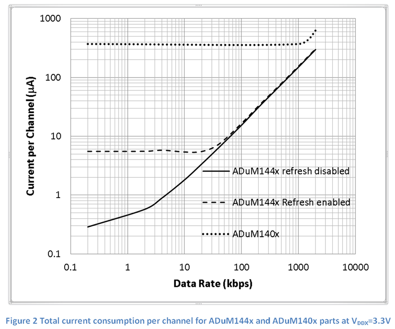
The current consumption as a function of frequency is shown in Figure 2 compared to the ADuM140x. The knee in the curves due to refresh can easily be seen at 1Mbps for the ADuM140x and at 17kbps for the ADuM144x when refresh is enabled. The ADuM144x has a typical current consumption per channel 65 times lower at 1kbps, and about 1000 times lower if refresh is completely disabled.
Click image to enlarge
Why is this much reduction in power useful? Below are three applications where traditional optocouplers and digital isolators are either marginal or completely unusable.
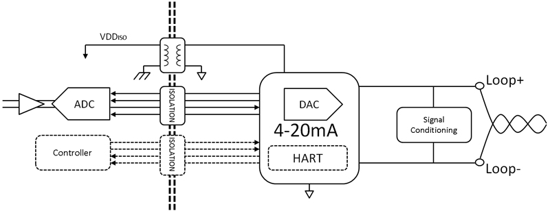
4mA to 20mA isolated loop-powered field instrument
Loop-powered field instruments (see Figure 3) have a very limited power budget since all power is derived from the 4mA loop current. Luckily the loop usually provides enough voltage, typically 24V to pull about 100mW from the system. The entire application will use about 12V of the loop voltage at 4mA. Within that budget a simple DC/DC converter supplies the isolated sensor ADC and controller.
Click image to enlarge
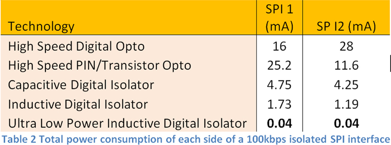
Even assuming a fairly high efficiency for the DC-DC converter, and a 2:1 step down in voltage, a typical sensor front end will have <4mA at 3.3V to work with, the loop side has about the same power budget. The primary interface is the SPI bus to the ADC. Each side of the isolated interface is powered from the loop along with all of the controllers ADCs and signal conditioning elements. Table 2 shows the current consumption for a 4 wire SPI bus for each of the isolation technologies. SPI 1 is the loop side current of the isolation, and SPI 2 is the sensor side current required. The optocouplers would consume many times the power budget on each side of the isolation interface.
Click image to enlarge
The capacitive digital isolator would consume the entire power budget for the field instrument. The ADuM1401 is a possibility, but the power budget for the rest of the system is marginal even when supporting only the single SPI interface to the ADC. The new ultra low power ADuM1441 iCoupler based digital isolator has such low power that it becomes a minor part of the power budget. This technology not only allows the application to work within its power budget, it allows the addition of a second 4 channel isolator to support a HART modem interface and a smart front end controller, shown in the dotted blocks of the diagram. The ultra low power iCoupler technology enables new functionality that was previously not possible to achieve in an isolated application.
Power Over Ethernet I2C Communications Bus
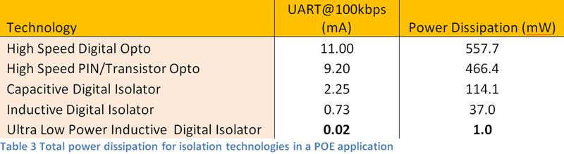
Telecom type applications like Power over Ethernet (POE) get power from a relatively high voltage rail, which supplies the Ethernet power. The control communications interfaces must get their power from an isolated DC/DC converter or through a regulator from the -54V bus voltage. In the example in Figure 4 the 3.3V communications interface for an I2C control bus is generated by a regulator internal to the POE controller. Table 3 shows the current required to run the I2C bus interface on the POE controller side along with the power dissipated inside the POE controller to support each technology.
Click image to enlarge
Click image to enlarge
An optocoupler solution would dissipate half a watt of heat inside a chip that is likely running close to its thermal limit already. Each interface is a bit better going down the table until we get to the Ultra low powerADuM1441 where the power dissipation is about 1mW. This makes the interface a trivial thermal load for this chip. Even if the power was not regulated internal to the POE chip, this power is so low that a simple Zener diode and resistor could be used to give a suitable supply saving component cost and cooling load. This technology simplifies power architectures.
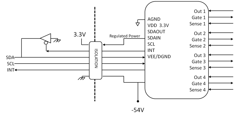
Battery powered medical sensor
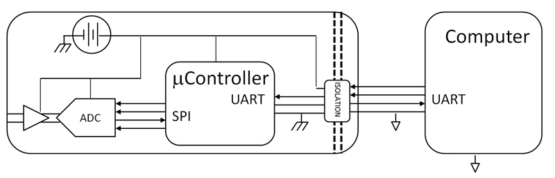
The third example of the use of ultra low power is to support long duration battery applications. Medical appliances such as glucose meters and pulse oximeters for home health monitoring must be constructed to allow contact with the patient and connection to a non-medical grade computer simultaneously (see Figure 5). The serial interface has to be powered and ready to wake up the device when the computer is connected, so an active isolator should be part of the standby circuit. In this case using the refresh disable feature of the ADuM1441 will allow the part to draw less than 4μA from the battery. This level is low enough that even a coin cell could maintain that standby current for years.
Click image to enlarge
The ultra low power of the ADuM1441 also allows convenient powering of the computer facing side of the isolation. With only a few μA of current to operate the interface, a status line in the serial interface can be dedicated to providing power to the isolator, so no dedicated power supplies are required.
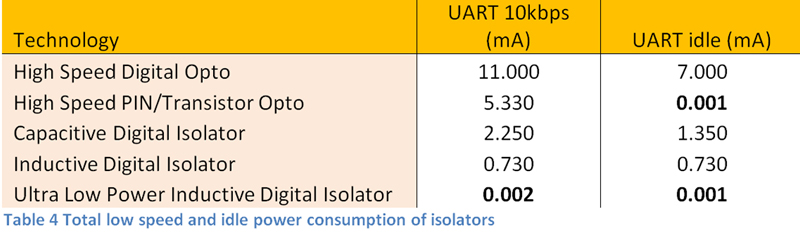
Table 4 illustrates some of the properties of optocouplers as well as the various varieties of digital isolation when operated in standby mode. Note that if the proper idle state is chosen, the PIN/transistor isolator can actually have a standby current as low as the ultra-low power iCoupler based product. This property of optocouplers has been used to generate low power standby in many applications. However, once communication starts the power consumption jumps to relatively high levels, which is not the case with the ADum1441 solution.
Click image to enlarge