High Voltage GaN Transistors for Speed and Efficiency
Why GaN Transistors?
Figure 1: Doped silicon transistor cross section compared to GaN HEMT
The high electron mobility transistor (HEMT) is a relative newcomer in the world of mass-produced power switching devices. Unlike its traditional doped Silicon counterpart, HEMTs are heterojunction devices built using two semiconductor materials with distinct bandgap voltages. First demonstrated in the late 1990s and early 2000s, HEMTs make use of a unique band diagram that results in a conceptual gas of majority electron carriers within the undoped low bandgap material. The resulting structure enables operation at extremely high frequencies due to the lack of scattering dopant atoms. The exact characteristics of the HEMT are dependent on the constituent materials, and can be tailored for either higher frequency or higher power applications. For example, Gallium Nitride (GaN) HEMTs, shown in the figure below, are particularly well suited for voltage converter applications and other high power switching topologies due to their extremely low on-state resistance.
In extremely high power applications, especially when frequencies are low, insulated gate bipolar transistors (IGBTs) have commonly been used. More recently, Silicon Carbide (SiC) MOSFETs have gained traction in this high power space, offering increasingly high frequency switching up to a several hundred KHz boundary. As shown in the figure below, when even higher switching speed is required at moderate power levels below 1000VA, HEMTs are the only viable solution. Some common examples of this requirement include power supplies for data center servers, consumer AC adapters, automotive 48V DC/DC converters, and LIDAR laser drivers.
Click image to enlarge
Figure 2: Power and frequency application space for IGBT’s, SiC MOSFETs, and GaN HEMTs
One of the greatest challenges in regard to the widespread adoption and mass production of GaN HEMTs over the last two decades has been the difficulties associated with gate driver design. The complex circuit requirements and the associated reliability issues demanded a solution before GaN HEMTs could gain any traction in the market. ROHM solved these problems by offering a dedicated gate driver chip series to simplify circuit design and ensure the highest performance. With these developments, GaN HEMTs from ROHM were ready for prime time, and the stage was set for the next act of developing even higher voltage devices.
GaN HEMT Applications
The sweet spot of GaN HEMT operation is characterized by very high frequency switching and moderately high power levels. This combination leads to a very specific set of application spaces that are growing more important every day, and are gaining commensurate market share of the electronics industry. Three of the most common examples are AC/DC converters such as AC adaptors and on-board chargers, DC/DC converters (i.e., 48V input, 12V output), and LiDAR.
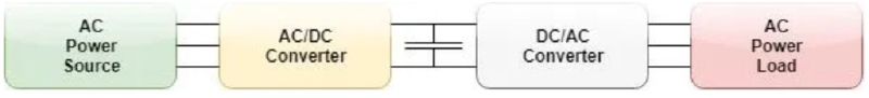
Motor drives are typically built from a series of voltage converters. As shown in the figure below, an AC source is first converted to high voltage DC, and then converted back to a variable frequency or variable voltage set of AC waveforms to drive the motor itself. In an electric vehicle, the high voltage DC bus could be used directly.
Click image to enlarge
Figure 3: Motor drive block diagram
The final DC/AC output stage is an ideal application for GaN HEMTs where the switching frequency might hover between 40 kHz and 100 kHz and the load currents can be substantial.
When compared to other technologies like silicon MOSFETs and IGBTs, GaN HEMTs are more efficient, more compact, and generally less expensive to implement.
Another GaN HEMT application gaining broad market visibility is the laser driver stage for LiDAR systems, particularly those used in autonomous driving applications. To create pulses of light for LiDAR, these lasers must be driven by a semiconductor switch. The quality of the switch directly affects the resolution of the LiDAR image, and is typically characterized by turn-on time, peak current, and switching loss. Compared to traditional silicon devices, GaN HEMT switches exhibit extremely fast speeds and up to 65% lower power loss. This yields enhanced LiDAR performance in terms of image quality while simultaneously improving efficiency and thermal complexity.
The market for GaN devices in RF applications is expected to reach $2 billion by 2024. Much of this is driven by radar applications, along with the development of shared electronics and antennas, for example electronically scanned array systems. Radar is commonly implemented using a high power, wide band traveling wave tube (TWT). GaN HEMTs are quickly replacing this unreliable, short operational life device through the application of pulse RF signals. As with the previous examples, the GaN HEMT solution yields higher reliability, improved efficiency, and better high frequency response.
Discrete High Voltage GaN
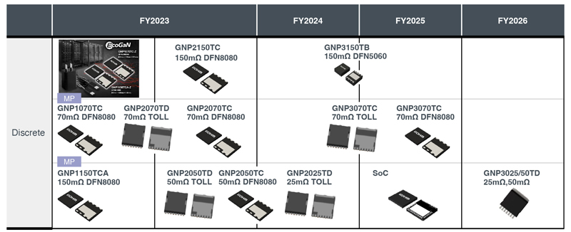
The ability to switch high voltages is critical for both size and efficiency. For the same power, higher voltage tolerance will yield lower current, in turn reducing on-state losses and minimizing physical device size. Overall, the higher voltage HEMT will have greater application across a wider variety of power supply topologies and offer competitive advantages in size and performance. To this end, ROHM has further developed its HEMT voltage capability to include discrete GaN devices up to 650V, and plans to roll out a broad portfolio over the next 4-5 years. As shown in the figure below, these high voltage transistors are trending toward lower on-state resistance and smaller, design friendly DFN packages. They all feature a high drain-source voltage tolerance of 650V, extremely fast switching times, and zero reverse recovery time.
Click image to enlarge
Figure 4: ROHM’s high voltage roadmap through 2026
ROHM’s lineup of GaN devices also features integrated ESD gate protection in every package, making them incredibly robust while simplifying the gate driver circuit design and minimizing component count.
HEMT Power Stage Devices
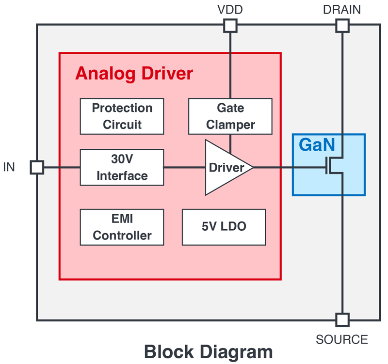
In addition to discrete GaN HEMTs, ROHM offers specialized power stage devices with integrated gate drivers. As shown in the figure below, the power transistor, the driver circuit, supporting circuitry, ESD protection, and EMI management are manufactured in a single package. This not only saves space, but also improves efficiency and enhances environmental immunity including thermal robustness.
Click image to enalrge
Figure 5: Power stage IC combining GaN HEMT and gate driver
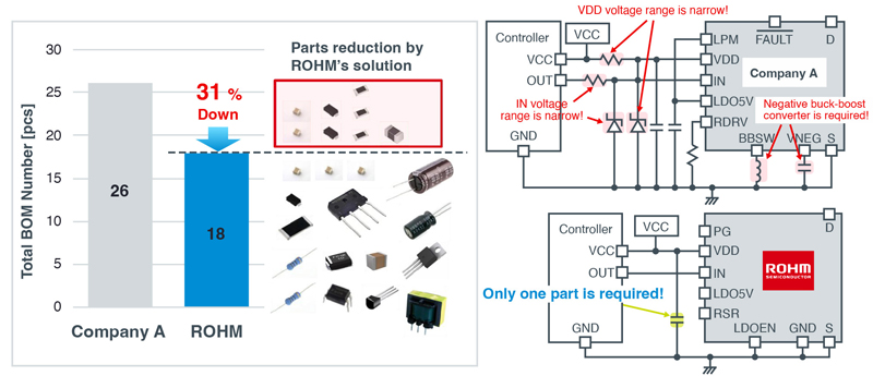
ROHM’s BM3G015MUV-LB and BM3G007MUV-LB are its flagship power stage devices, and feature a wide input voltage range of 2.5V to 30V, an extremely low 15ns propagation delay, adjustable slew rate, and low quiescent current. These devices are particularly well suited for a variety of power supply switching topologies, including flyback, LLC, interleaved PFC, and totem-pole PFC. As shown in the figure below, taking advantage of ROHM’s integrated power stage devices reduces part count for a representative circuit by 31%, and improves voltage performance while also minimizing physical volume. This also enhances thermal performance by enabling the designer to optimize the PCB with greater freedom, and gains of up to 25% in total output power have been measured in common power supply designs.
Click image to enlarge
Figure 6: BOM advantage using power stage devices
HEMT System In Package
Similar to the power stage devices, ROHM’s system in package (SIP) products integrate multiple parts of a complex system to reduce part count, simplify design, and enhance functionality. SIPs are typically application specific and contain parts selected and optimized for a particular design topology. For example, ROHM is developing several high voltage GaN SIPs for flyback voltage converters (BM3GQ12A3MUV-LB and BM3GQ12A2MUV-LB) and PFC power supplies (BM3GF01MUV-LB and BM3GF02MUV-LB). These SIPs include the power GaN HEMT, the gate driver, sensing resistors, supporting amplifiers and LDOs, along with a variety of other controls and utility functions.
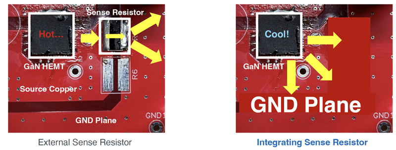
Again, reducing the discrete part count enhances freedom to optimize the thermal performance of the PCB, which in turn boosts the overall system performance. As an example, a PFC converter SIP with integrated sense resistor is shown in the figure below. In addition to the reduced BOM complexity, the enhanced ground plane surrounding the SIP offers a significant cooling advantage.
Click image to enlarge
Figure 7: Thermal advantage of using SIP with integrated sense resistor
Conclusions
Recent advancements in ROHM’s EcoGaN transistors have yielded a broad portfolio of power HEMTs and an extensive roadmap for future development. From 650V discrete transistors to complex power stage and SIP products, ROHM has provided a foundation for HEMT adoption across the gamut of high frequency power applications. Their 650V GaN HEMT has achieved the industry's highest class FOM (Figure of Merit), offering unparalleled switching loss reduction when compared to conventional GaN devices and contributing to the industry-high levels of power supply efficiency.
ROHM has developed a manufacturing solution for its GaN devices, starting with the raw wafer creation and ending with the final product packaging, that guarantees the highest levels of quality while also ensuring a stable and predictable supply chain. In the development of all of its products, ROHM promotes strategic partnerships to contribute to solving social issues by making applications more efficient and compact.