Ideal for industrial input voltage range
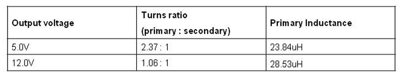
Table 1: Turns Ratios and Inductances
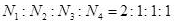
For industrial applications, power supplies with galvanic isolation in the range of 10 to 20W are often required. In general, a flyback converter is a good choice for this application. But when the output voltage is low as 5V for example, higher output currents cause significant losses on the rectification diode. It decreases not only efficiency but generates heat, which has to be dissipated. This article introduces the design of a flyback converter with industrial input voltage range (9-36V) and low-cost synchronous rectification on the secondary side to achieve high efficiency even at higher output currents. Furthermore, the design procedure for a transformer is shown, where a single transformer with two output windings is used for a power supply with 5V or 12V output voltage at the same power level. Design of the transformer Specifications of the power supply: • Input voltage range: 9-36V DC • Output voltage: 5.0V @ 4.0A or 12.0V @ 1.5A • Galvanic isolation & high efficiency • One transformer for both output voltages To start with the calculations, at first the switching frequency has to be selected. It is well known that the transformer size gets smaller when increasing the switching frequency. But the higher the switching frequency, the more dominant are the switching losses. So it is better to stay at a relatively low value of 200kHz as the transformer will still be small enough at approximately 20W. Texas Instruments "Power Stage Designer™ Tool" is very helpful when designing a flyback transformer. You can quickly figure out the required inductance, turns ratio and current load for the specification needed by the transformer manufacturer. To reduce design time, this tool is used to specify the custom made flyback transformer. Needless to say that all calculations can be done also by hand as described in various books and application notes. At this power level the converter should work in continuous conduction mode and with a maximum duty cycle around 60% to prevent high peak currents during demagnetization. A current ripple of 40% is feasible, because a flyback converter needs plenty of output capacitance anyway. The additional post-filter reduces the voltage ripple further. For a 5.0V or 12.0V output with the specification above, the tool recommends the following turns ratios and inductances: One solution could be to use the same turns ratio for both output voltage or to choose the average of both values, approximately 1.7 : 1. In all cases the maximum duty cycle of 60% is exceeded or the duty cycle gets very small which increases the stress on the parts due to high peak currents. The better solution is to use a transformer with multiple windings, which can be paralleled or put in series to achieve a turns ratio close to the calculated values. The primary inductance is almost the same for both output voltages, so a value of 25uH is chosen. With the primary side fixed with one winding, two separate windings are needed on the secondary side. It must be possible to get a ratio of 2:1 and 1:1 with these three windings. This can be achieved by using the following turns ratio:

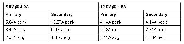
Putting the two secondary windings in parallel results in a turns ratio of 2:1 and putting them in series gives a ratio of 1:1. This fits almost perfect for the specification. The next step is to figure out the maximum rms and peak current in each winding for the two different turns ratios. Again, "Power Stage Designer™ Tool" makes things easy. The table below shows the current stress in each winding: The highest currents occur in 5V configuration. Given that the two windings are in parallel, each winding has to be designed for 5A peak and 3A rms. These ratings meet the requirements for the 12V configuration as well.
.jpg)
Implementing synchronous rectification At this current level a diode rectification on the secondary side, as it is used in most flyback designs, causes significant losses (approx. 1-2W) which reduces not only efficiency but also can cause problems to dissipate the heat. This can be avoided by a synchronous rectification as it is used in a lot of other topologies like buck converters. Therefore, the diode is substituted by a MOSFET and controlled with a signal, which has to be inverse to the gate signal of the primary side MOSFET. When the primary MOSFET is switched on, the MOSFET on the secondary side has to be switched off and vice versa. The gate signal of the primary side MOSFET can be used for this, but is has to be transferred to the secondary side by an optocoupler or gate transformer to keep the galvanic isolation. Another possibility is to add an additional winding on the secondary side of the transformer which drives a MOSFET for synchronous rectification. This is a so called "self-drive synchronous rectification". Figure 1 shows the simplified schematic of such a power stage in 12V configuration. N1 is the primary winding, which is attached to the input voltage. N2 and N3 are the two secondary windings, which are connected in series for a 12V output or in parallel for a 5V output. Winding N4 is just stacked onto the output winding generating a voltage higher than the output voltage to drive the secondary side MOSFET. Therefore, it can be rated for a much lower current. The turns ratio of the windings is as follows:
The minimum and maximum voltage on the gate of MOSFET Q2 is calculated with Equation 3 and Equation 4:
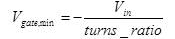
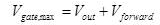
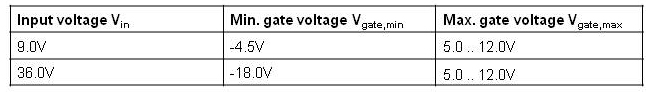
Vforward is the forward voltage drop of the rectification diode. In this design the diode is substituted by a MOSFET, so it can be neglected. As the ratio between the primary winding N1 and the rectification winding N4 is fixed to 2:1, the minimum gate voltage is independent of the output voltage configuration. Unlike that, the maximum gate voltage equals always the output voltage. In theory, MOSFET Q2 could be directly connected to winding N4. The minimum and maximum gate voltage from the table above are within specification of most MOSFETs (�20V). Due to the leakage inductance of the transformer ringing and overshoots can be measured on all windings of the transformer. So it is necessary to control the gate voltage with additional circuitry to protect the MOSFET as it is shown in the schematic. The 15V bi-directional suppressor diode D1 between gate and source limits the driving voltage from the transformer. Resistor R1 is needed to allow a voltage drop when the diode is clamping. The resistance shouldn't be too high, otherwise the switching speed of MOSFET Q2 is reduced leading to higher switching losses and therefore less efficiency. A snubber circuit (R2, C2) across drain and source reduces ringing and spikes to improve EMI behavior. With different in-/output voltages and turns ratios the calculated gate voltage can be lower or higher than the maximum ratings of the selected MOSFET. In that case it is not recommended to use a synchronous rectification with such a simple driving circuit. The used suppressor diode clamps the gate-source voltage to a maximum/minimum of �18.5V. All additional voltage drops on the low-resistive resistor R1, which acts as a current limiter. This current flows also through the suppressor diode and causes excessive losses (Psuppressor = 18.5V * IR1). Therefore designs generating higher gate voltages need a modification of the driving circuit to avoid this problem.
.JPG)
Measurements Figure 2 and Figure 3 show the efficiency of the 5V and 12V output configuration. To achieve the best results, different MOSFETs for the rectification were selected.
.JPG)
.jpg)
The drain-source voltage of the secondary side MOSFET in 5V configuration at 36V input voltage and a load of 4A is plotted in Figure 4. The high overshoot can be reduced further by harder snubbering at expense of efficiency.
.jpg)
The according gate-source voltage in Figure 5 is clamped by the protection circuit well above -20V. The driving voltage with approximately +5V is enough for this MOSFET. When selecting a MOSFET, not only care of the breakdown voltage and the gate charge should be taken, but also of the minimum gate threshold to ensure a proper switching with the calculated maximum voltage on the rectification winding. Conclusion With two independent windings a single flyback transformer can be used for 5V or 12V output at the same input voltage range. An additional winding extends it for synchronous rectification to improve efficiency at higher output currents. The introduced transformer was built by Würth Elektronik (part number 760372002) and is available for all customers. The flyback converter is designed for industrial input voltage range (9..36V DC) and delivers around 20W in both configurations. The two designs were built and tested, all information (schematic, bill of material, test report, gerber files) can be downloaded on TI.com under the keyword "PMP4626". Downloads 5V version: http://focus.ti.com/docs/toolsw/folders/print/pmp4626.1.html 12V version: http://focus.ti.com/docs/toolsw/folders/print/pmp4626.2.html Power Stage Designer™ Tool: http://focus.ti.com/docs/toolsw/folders/print/powerstage-designer.html www.ti.com