Silicon MOSFETs have been used in parallel configurations in power converters for many years, but GaN power transistors are still a novelty for many engineers.
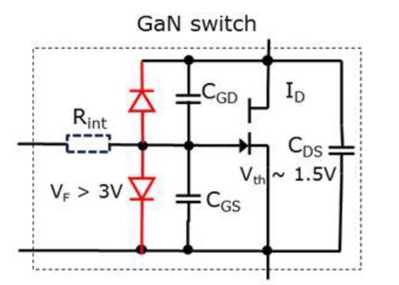
Figure 1a: E-mode GaN HEMT equivalent circuit
Wide-bandgap (WBG) technology is increasingly becoming an alternative to traditional silicon MOSFETs in power converters. In market segments where the remaining percentage point or two of efficiency can really make a difference or an increase in power density can provide an advantage, a move to gallium nitride (GaN) transistors can make a lot of sense. Just as with silicon, there is a practical upper limit to how large a die can be manufactured in GaN and, therefore, an upper limit on the current-handling capability of a single device. To increase output power, the paralleling of switching devices has been one of the options open to design engineers. While this can increase the current capability by almost the maximum continuous current for each additional switch, a plethora of design challenges arise as a result.
The challenges of using switching devices in parallel
When operating switching devices in parallel, the first concern relates to the RDS(on) of the devices used. Ideally, the selected devices should be evenly matched to ensure that the static current flowing is shared equally amongst the parallel switches. The second concern relates to the dynamic switching. Lack of symmetry at the gates of each switch can not only result in an imbalance in current sharing across the devices; the flow of current combined with circuit parasitic effects can also result in undesirable high-frequency oscillations. This can result in challenges fulfilling EMC requirements, or even cause destruction of the switches if left unresolved.
While the parallel operation of silicon MOSFETs is well understood, the driving of single GaN HEMT devices is still uncharted waters for many. This, coupled with their exceptionally fast switching speed, means that a thorough understanding of these power transistors should be attained prior to tackling the challenges of operating them in parallel.
Getting the drive right
Devices such as the Infineon CoolGaN 600 V HEMT make use of p-doped GaN beneath the gate. This shifts the device’s threshold voltage to a positive value, although this is typically quite low lying at around 1.0 V to 1.5 V. This results in the gate forming a pn-diode with a forward voltage of around 3.0 V and resistance of a few Ohms. As a result, the drive circuitry is quite different from that used with a classic MOSFET.
The gate input of a CoolGaN transistor can be thought of as a diode with a forward voltage, VF, of around 3.5 V in parallel with the gate’s capacitance, CG. It is the diode that makes driving these devices challenging as, once the Miller plateau has been reached, the gate node is clamped to a value close to VF. This means that a negative voltage is required to turn the transistor off in a hard-switched application. There is also a difference in the drive needed between steady on-state and during off-/on-transients.
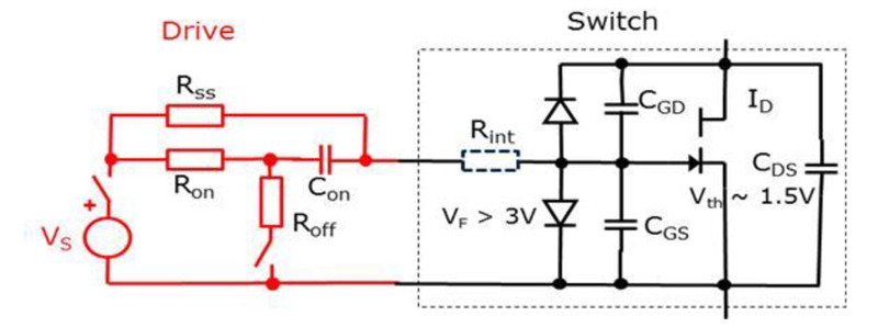
This is resolved by using the circuit shown in Figure 1. Ron provides a low-impedance fast AC-path to charge Con and CGS. To ensure this occurs, the drive voltage, VS, needs to peak at more than twice the VF (8 V to 10 V is commonly used). A parallel DC path is then formed through RSS. Thus, if dimensioned correctly, the on-transient current is defined by Ron, while RSS determines the steady-state diode current.
When the gate is turned off, a fast balancing of the charges in CGS and Con takes place. Here it is necessary to ensure that Con is larger than CGS as the resultant difference in charge will cause the gate voltage, VG, to go negative, thereby turning the transistor off in hard-switched applications.
Click image to enlarge
Figure 1b: Proposed driving scheme
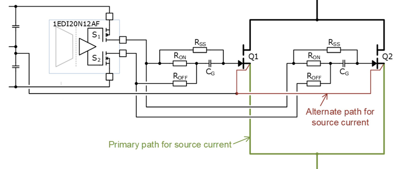
When operating CoolGaN HEMTs in parallel, this same RC driving network can be used with the gate of each transistor in combination with standard gate drivers that are commonly in use in silicon MOSFET applications. It requires a single gate driver, such as the isolated EiceDRIVER 1EDI20N12AF, using the source (OUT+) and sink (OUT-) outputs to separately implement the turn-on and turn-off of the transistors. When using an isolated 12 V supply for the gate driver, this is split into a positive and negative supply with the negative supply regulated at -2.5 V. This ensures that the transistor gate threshold is not exceeded and helps to minimize reverse conduction losses. It also keeps the gate voltage well defined, even at low duty-cycles, stopping the RC driving network tending towards 0 V.
The impact of alternate current paths
Even with separate RC drive circuitry for each transistor, there is still a shared current path that will interfere with the gate driver loops (Figure 2). Ideally, all current would flow through the intended path from drain to source but, inevitably, some flows through the Kelvin source path. Should these paths not have identical impedance and routing, different VGS voltages in the CoolGaN HEMT gate loops can result. A few mV of difference at the gate can result in several amps of unbalanced current sharing, along with severe oscillations during switching events between the two transistors.
Click image to enlarge
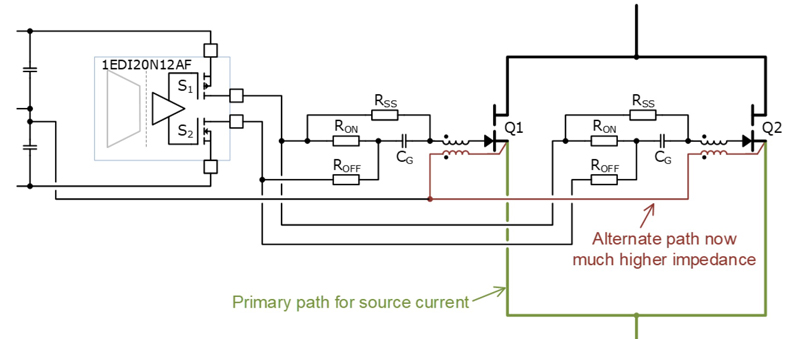
Figure 2a & 2b: In parallel CoolGaN operation, a high impedance in the Kelvin source path keeps severe oscillations in check
The introduction of a high-impedance common-mode (CM) path in the Kelvin source path resolves this issue. CM inductors placed between the gates and the corresponding Kelvin source driver return path, together with a 1 Ωresistor, result in the gate-drive loop only seeing a small leakage inductance. The shared current path, on the other hand, now sees the full differential CM inductance of both inductors. Careful selection of the inductor is required to avoid compromising the capability of the gate driver. The impact of the CM inductors is clearly shown, as a result of a SIMetrix simulation, in Figure 3.
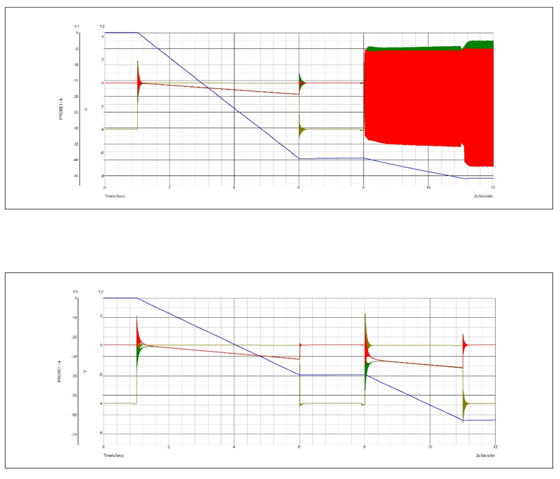
Click image to enlarge
Figure 3: Simulation showing the impact of switching 40 A without CM inductors (above) and with CM inductors (below)
Good practice PCB design
Another common concern when operating devices in parallel is the impact of stray inductances and capacitances in the PCB (layout, traces, layer arrangements) together with those of the component used. With respect to the CoolGaN™ HEMTs, the key concern is the impact caused by the range of VGS threshold values and differences in RDS(on) between transistors. Simulations undertaken in SIMetrix with transistor models, using threshold voltages of 0.9 V to 1.6 V and RDS(on) values of 55 mΩ to 70 mΩ, have been undertaken to investigate this. In addition, the impact of trace inductances and layer capacitances were also modeled.
The results of this analysis showed that the static imbalance in current sharing is related solely to differences in RDS(on) between the transistor used. This can be resolved by undertaking device matching if deemed necessary. Destructive sustained oscillations are eliminated by the use of the CM inductor, as previously stated. However, following good layout practice is also a key factor. Power loops and gate-drive loops must be kept small and symmetrical, while also ensuring that the switch-node parasitic capacitance is kept as low as possible.
Collecting practical experience
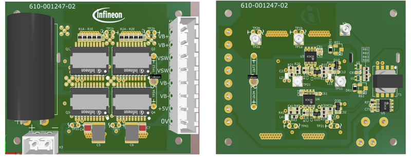
The optimal way to understand the challenges and their solutions is by undertaking experimentation in the laboratory. For this purpose, Infineon has developed a parallel half-bridge evaluation board that features four 70 mΩIGOT60R070D1 GaN power transistors. It follows the design guidelines discussed here, providing an excellent starting point for both evaluation and design development. It also offers plenty of test points for full analysis. An important point to note is the need for high-bandwidth, isolated, differential probes for some measurement points, and the requirement to ‘de-skew’ for accurate channel timing prior to use.
In conjunction with an external inductor, the board can be used for buck or boost mode tests, double-pulse testing, and pulse-width modulation (PWM) operation. It is also suited to both hard- and soft-switching at power levels of several kW and frequencies of up to 1 MHz. The pluggable terminal block simplifies reconfiguration of the test setup, while a further connector allows a capacitance to be added in addition to the on board 100 µF, 450 V bulk capacitor. This component, along with two further high-frequency bypass capacitors, defines the output or bus voltage limit of 450 V. The evaluation board can operate at a continuous current up to 28 A, and a peak current of 70 A during hard- or soft-switching, provided that appropriate heatsinking, thermal interface material, and airflow are used. Potentiometers in dead-time circuitry are included to implement delayed turn-on via an RC network, and non-delayed turn-off via a diode.
Click image to enlarge
Figure 4: Parallel half-bridge CoolGaN evaluation platform
Summary
The different approach to drive GaN transistor gates is the first step to mastering their use. From here, their use in parallel operation is relatively straightforward, but should not be considered as simplistic. Balancing of the currents between the devices under static conditions, and following best practice in PCB layout, both require informed attention during the design phase. Finally, the use of correctly dimensioned CM inductors in the gate and Kelvin source path is an essential aspect that will help to keep the potential for destructive oscillations under control.