The trade-offs to be made in design choices, between a device’s performance, cost, operating requirements, size, thermal efficiency and availability
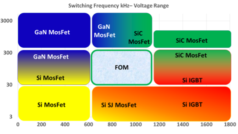
Figure 1: Appropriate operating regimes for various devices types
Every engineer wants a perfect switch that flips between On and Off states instantaneously and which doesn’t suffer losses in either state. To achieve the lowest possible losses when switching between the two states relies on the switch having a number of characteristics. It needs to have an infinite breakdown voltage, not to allow any current to flow when it is Off, not to sustain a voltage difference across it when it is On, and not to take any time to turn On or Off.
Such a switch doesn’t exist. Real switches have a finite breakdown voltage, leak current when Off, sustain a voltage across them when On, and take measurable amounts of time to switch between states. And all real switches will always dissipate some power, both when On and during switching.
New technology broadens switching options
However, new materials technology, in the form of wide-bandgap semiconductors such as silicon carbide (SiC) and gallium nitride (GaN), is providing options that improve circuit designers’ options and bring us closer to that ideal switch. As usual with new technologies, there’s a price to pay for these advantages but this is often offset by savings made possible elsewhere in the circuit design, as well as the increased commercial value of improved performance.
For example, it’s much less expensive to grow Si wafers than SiC ones, because the manufacturing process is much better optimised for volume production. Cutting, grinding and polishing SiC wafers also takes longer than Si because SiC is harder. Nonetheless, the extra expense can be worthwhile, because wideband-gap materials have useful properties.
Some questions about making the right design trade-offs around using these new devices almost answer themselves. It obviously doesn’t make sense to replace a Si MOSFET with a SiC MOSFET in a 3-euro plug-top power supply. But it might be worthwhile to use a SiC diode instead of a silicon epitaxial diode to improve the supply’s power factor correction (PFC). This would improve its conversion efficiency by 1% or 2% and also provide what could be very welcome extra margin for the thermal and mechanical designers.
Does it make sense to substitute a SiC MOSFET for a Si device? In some cases, yes, if you can adapt the circuit’s driver stage to deliver a higher gate-on voltage and to cope with a gate-off voltage that may sometimes be negative. Gate-driver devices are already available to match the required driver stages and transistors. The upside of making this change is that it allows the switching frequency of the design to be increased three- or five-fold. This in turn saves space by enabling the use of smaller magnetic components and other passives.
Is it worth paying for the relatively high, 175 to 200°C, operating temperature of SiC? Yes, if you can use the higher thermal margin to upgrade the specification of your device and sell it into a new market, or to reduce the size of the heatsink and so shrink the final product.
This high operating temperature range may also be an attractive option for some industrial and automotive applications. However, these markets can be conservative about their uptake of new technology because they need it to have a very long operating lifetime. Some SIC device suppliers are addressing this concern by introducing tests, such as the ‘dynamic H3TRB high-temperature high-humidity reversed bias’ test, to demonstrate that their parts are of similar quality to traditional Si alternatives.
And what about GaN devices? Where do they make sense? At the moment GaN technology is being used to make 650V devices for single-phase grid-powered applications such as switch-mode power supplies, chargers and adapters; high-voltage PFC; DC-DC and DC-AC converters; UPS systems, and smaller solar inverters.
Figure 1 maps out the appropriate operating regimes for various device types.
If you’re confused about choosing between the different types of semiconductor device and material, we’ve produced a simple methodology for doing so, which is outlined here.
Choosing devices based on the operating conditions
Which semiconductor device should we use in power-switching circuits, based on their operating conditions?
Let’s take, as an example, the design of an H-bridge as part of an AC-DC converter. The DC bus voltage is 370V, the current in the transformer is about 3A, and the switch runs at 15 to 25kHz. For safety reasons, we choose a component that can sustain 650V switching and a continuous drain current of at least 30A. We don’t have any glue logic, and plan to use either a silicon insulated gate bipolar transistor (IGBT), a silicon superjunction (SJ), a SiC or a GaN device.
Click image to enlarge
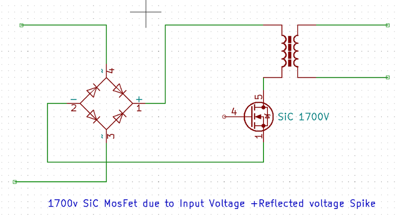
Figure 2: Simple example of a SiC MOSFET in a 100W auxiliary power supply
One way to choose which device to use is to focus on its operating conditions. We can make our choice by answering a series of questions about these conditions:
· Will the circuit design switch at less than about 20kHz?
· Is the power level above 3kW?
· If low cost is important, is the device low cost?
· Will the design be supplied by a three-phase grid?
If the answer is ‘yes’ to any of the above, then the best option is a Si IGBT.
If the design doesn’t fit these criteria, then the next set of questions will help narrow the choice:
· Is the switching frequency between 20 kHz and 100kHz?
· Will the design operate under a wide variety of line and load conditions?
· Does the design need high efficiency at moderate cost?
· Will the design be powered by a single-phase grid?
If the design meets these characteristics, then the best device option is a Si SJ MOSFET.
If the design does not meet these criteria, then we can move on to ask:
· Is the switching frequency above 100kHz?
· Will the design operate under a wide variety of line and load conditions?
· Is this a high-power design, operating at up to several kWs, which will require high efficiency?
· Is the design supposed to allow power to flow in both directions?
· Will the design be supplied by a three-phase grid?
If these conditions apply, then the best choice of device is a SiC MOSFET.
If we still haven’t found our device, we should ask:
· Will the design’s switching frequency above 100kHz and in the MHz range?
· Will it operate under a wide variety of line and load conditions?
· Is the design supposed to support medium power levels, of up to several hundred watts, with the greatest power density and efficiency?
· Will the design be supplied by a single-phase grid?
If the design does meet these criteria, the best option may be a GaN MOSFET.
Choosing a device based on the target application
Again, we can work through a set of criteria to define which device to use. In general, motor drives operating at more than 250W, power factor correction (PFC) circuits operating at more than 3kW, solar/wind inverters running at more than 5kW, and UPS and welding H-bridge inverters, should be designed around Si IGBTs.
Click image to enlarge
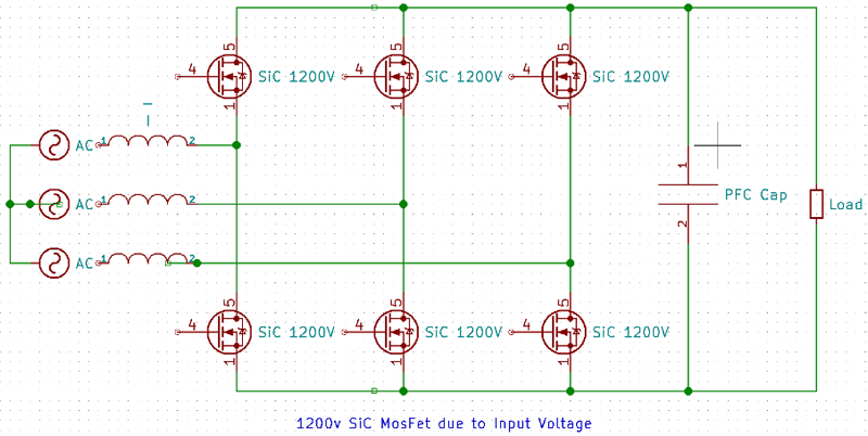
Figure 3: A mid-complexity 10kW sixpack PFC converter for AC-DC applications
For motor drives operating at less than 250W, DC-DC converters operating between 75W and 3kW, low- to mid-power PFC circuits and LCC converters, forward-converter power supplies, universal input AC-DC flyback circuits, and solar micro-inverters should be built using Si SJ MOSFET.
Higher power designs, such as PFC circuits operating at more than 3kW, solar inverters operating at more than 5kW, some electric vehicle and onboard chargers, as well as some uninterruptible power supplies and embedded PFC circuits, should be built using a SiC MOSFET.
Click image to enlarge
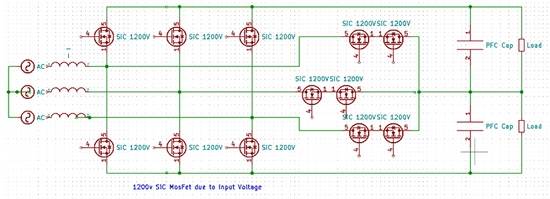
Figure 4: A complex bidirectional active PFC converter for AC/DC applications, inverters or electric vehicle on-board chargers, with power-return functionality
Finally, applications that are powered from a single-phase grid line and operate at less than 650V, which operate at between 75W and 750W, and need to be small, cool and portable, should be designed around GaN MOSFET.
There are always trade-offs to be made in design choices, between a device’s performance, cost, operating requirements, size, thermal efficiency, availability, and so on. The introduction of Sic and GaN technologies may make exploring these trade-offs more complex by introducing further options, but in some applications, it could help your design’s characteristics move closer to those of that perfect switch.