How to create an I2C to UART converter using the GreenPAK SLG46855V or any other GreenPAK family member with the available resources
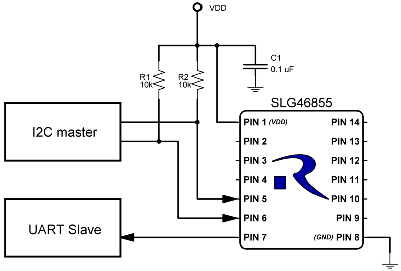
Figure 1. A block diagram of the connections between the I2C master, UART, and the SLG46855
The SLG46855V is a small package GreenPAK with a huge amount of digital logic and a wide supply range from 2.3 V to 5.5 V. There are a lot of flip-flops, lookup tables, and counter/delay blocks that can be configured to different functions. Flip-flops will be used to create a shift register, lookup tables as multiplexers, and counter/delay as a frequency generator. The design can be easily modified to use a different bus speed.
The Inter-Integrated Circuit bus, also known as I2C, is a very common bidirectional communication bus, that uses two lines to send serial information between devices. The bus is used in microcontroller systems for short-distance communication.
Basic I2C communication is using transfers of 8 bits or bytes. In a normal state, SCL and SDA lines are high. The communication starts with a start bit when the SDA line goes low while the SCL line is high. One bit is transferred during each clock pulse of the SCL. Data is transferred Most Significant Bit (MSB) first. Data on the SDA line must remain stable during the high phase of the clock period, as changes in the SDA line when SCL is high are interpreted as control commands (START or STOP bits). ACK bit takes place after every 8 bits. The bit allows the receiver to send a signal to the transmitter that these 8 bits were successfully received and another byte may be sent.
One of the features of the I2C protocol is clock stretching. A slave device can hold the SCL line low after receiving an abate indication that it is not yet ready to process more data. The master must wait until the SCL line goes high. Clock stretching is the only time when the slave controls the SCL line.
A Universal Asynchronous receiver-transmitter (UART) is one of the simplest communication buses which can be used for only one data line.
Basic UART communication is used to transfer 8 bits or bytes with a parity bit. In a normal state, the TX line is high. The communication starts with a start bit when the TX line goes low for one clock cycle. Data is transferred Least Significant Bit (LSB) first. After data bits transmit parity bit which describes the evenness or oddness of the transmitted byte.
Click image to enlarge
Figure 2. Smart Blind Controller Block Diagram
GreenPAK Design
The idea behind the design is to use SLG46855 to store 8 bits of I2C command and pull down the SCL line. The I2C master will stop transmitting if the SCL line is pulled down. Next SLG46855 will push these 8 bits to UART and then release the SCL line to receive the next 8 bits. Figure 1 shows the block diagram of the connections between the I2C master, UART, and the SLG46855 for this application.
The main problem is that the I2Cprotocol first transmits MSB and UART’s LSB. That’s why we need to save 8 bits in the shift register and push these bits in reverse order like stack memory. But I2C master and UART slave can have different bus speeds.
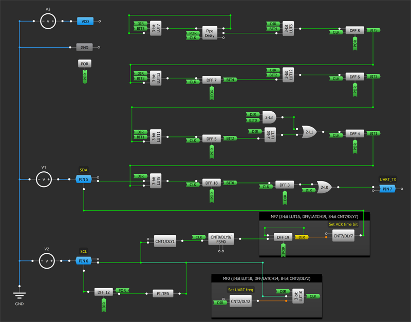
Input pins PIN5(SDA) and PIN6(SCL) are configured as digital input/output. They are used as digital in without Schmitt trigger when receiving I2C commands and as 1x open drain NMOS during transmitting UART commands. When the DIR signal is 1 the PIN6(SCL) is used as 1x open drain NMOS and pulls down the SCL line for clock stretching. At that moment I2C master stops transfer commands and waits until the SCL line will release. PIN5(SDA) is used as a digital output to transfer the acknowledging bit after every 8 bits.
DFF4-DFF8, DFF18, and Pipe Delay create a shift register and are used to store 8 bits. 2-bit LUT1-3, 3-bit LUT6, 3-bit LUT7, 3-bit LUT11-13, and 3-bit LUT8 are used to control the direction of the shift register. The design load 8 bits from the SDA pin if the DIR signal is ‘1’ and pushes these 8 bits when the DIR signal is ‘0’. In the default state, the DIR signal is ‘1’, and the design is ready to store data from the SDA line and SCL pin configured as a digital input. The design push bit from the SDA pin to the shift register on every rising edge on the SCL pin. The MSB bit from the I2C command stores in Pipe Delay. The bit goes from PIN5(SDA) trough 3-bit LUT8, DFF18, 2-bit LUT3, 2-bit LUT1, DFF4, 3-bit LUT11, DFF5, 3-bit LUT12, DFF6, 3-bit LUT13, DFF7, 3-bit LUT6, DFF8, 3-bit LUT7. When SLG46855 transmits the UART command the MSB bit goes in reverse order to PIN7(UART_TX). CNT0 uses to count the clock on the SCL pin and after 8 clock DIR signal goes ‘0’. When the DIR signal is ‘0’ the design pulls down the SCL line and the I2C master waits until the SCL line will release. CNT2 creates a CLK signal to push 8 bits from the shift register to UART_TX. You can change the UART baud rate using the I2C command. CNT2 counter data stored in register 0x9A. DFF3 is used to generate the start bit for the UART command. CLK signal defines the baud rate of UART. After the last bit will be pushed then DLY7 creates an ACK on the SDA line (pull down SDA line).

Click image to enlarge
Figure 3. Experimental Transmission
The complete design file can be found at www.renesas.com/cm-347-gp-file. It was created in free GUI-based GreenPAK Designer software – a part of Go Configure Software Hub.
To test the design, the I2Cmaster writes data 0x00, 0x01, 0x02, 0x03, 0x04, 0x05, 0x06, 0x007 to address 0x01.
The simulation results are divided into a few parts.
For Part 1, the I2Cmaster generates the start bit and transmits the write command for the slave with address 0x01. The design receives the data and pulls the SCL line to GND. On PIN 7, the user can observe the UART start bit and convert the slave address from the I2Cmaster. GreenPAK release SCL line and pulls SDA line to GND for ACK signal. I2Cmaster transmits the data 0x00 for part 2, data 0xAA for part 3 and 0xFF for part 4.
Conclusions
This article demonstrates how to create an I2C to UART converter using a GreenPAK IC. The design is limited to a message size of 8 bits. SLG46855 has a lot of digital resources in a small package that can be used to create unique digital designs.