A look at best practices for choosing the correct components and verifying the design of a variable output buck regulator
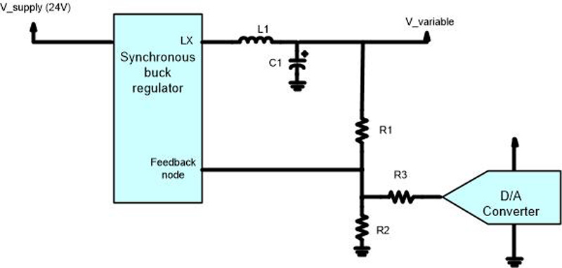
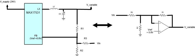
Figure 1. Example of a variable output buck regulator
There are numerous reasons for creating a variable output buck regulator, such as to control speed of a DC fan, set the voltage for a 4 – 20mA current loop, track another voltage, or for dynamic voltage scaling. The processes for choosing the correct components and verifying the design are examined here.
Figure 1 is a typical diagram for a variable output buck regulator created by summing the output of a digital-to-analog converter (DAC) into the feedback node. The DAC could be any voltage source.
This article highlights a three-step approach to design a variable buck. The article will share an example and provide some real-world measurements of the example design.
The three steps that will be used are:
1. Determine the voltage ranges required for the design and the proper buck regulator
2. Calculate the resistor network for the feedback node shown as R1, R2, and R3
3. Use an online design tool / simulator to choose the proper components and simulate the design
Determining the Voltage Ranges and Selecting the Proper Buck Regulator
In most cases there will be a rail available in the system that will be used as an input to the buck regulator. In this example, 24V was chosen since it is a common rail in industrial applications. The output voltage range now needs to be determined and some care needs to be taken at this point, since many buck regulators will have a limited output voltage range and also because component recommendations (such as Ls and Cs) will change based on the output voltage chosen. In this type of design, the components will remain the same over the full span of the varying output. Later, the example design will be checked for stability and step response at the highest and lowest output voltages using the online design tool/simulator.
This example used an output voltage range of 6V – 19V and an output current of 50mA maximum. Generally, buck converters that cover a wide range of input and output voltages are ideal for this type of application. Specifically, this example used a 50mA synchronous buck with a 4V – 60V input range and a 0.8V up to 0.9 x Vin output range.
For the controlling voltage, a DAC was chosen, but another variable source, such as a filtered pulse-width modulation (PWM) signal, could be used here. In this case, a 2mm x 3mm, 12-bit voltage output serial DAC with an internal reference was used. The DAC can be powered from a 2.7V to 5.5V supply.
With a 3.3V supply and the internal 2.5V reference, the output of the DAC can go from 0V to 2.5V under a 12-bit digital control. To control the variable supply, this example leaves a little headroom above 0V and below 2.5V to account for offset, gain, and inaccuracies in the feedback resistors. The full range of the varying output (6V to 19V) will be controlled from a 0.1V to 2.4V control signal. This leaves 100mV or about 82 DAC codes on either end if calibration or adjustment are required.
Calculating the Resistor Network
For the purpose of calculating the resistor values, it may be easier to look at the variable power supply circuit as an ideal op-amp circuit (Figure 2). Indeed, in this case, the supply is acting like an inverting amplifier where the DAC is the input signal (Vin). The 0.8V Vref shown is the internal 0.8V reference used with the error amplifier internal to the synchronous buck.
Click image to enlarge
Figure 2. Variable power supply circuit as an ideal op-amp circuit
To figure out the three resistor values in this way, use the following method:
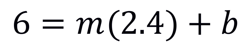
Assume that the switching supply Vout is responding linearly to the DAC input like an ideal op-amp and the input to output relationship is that of a straight line with the familiar equation:
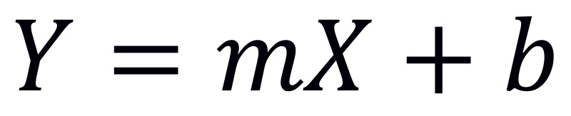
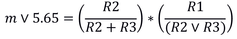
Here Y is the output voltage of the switcher (or op-amp) and X is the input voltage from the DAC (Vin). Using the two points (19Vout at 0.1Vin and 6Vout at 2.4Vin) gives two equations to solve for m (gain) and b (offset).

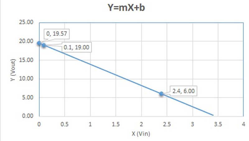
Solving this we get m (gain) = -5.65 and b (offset) = 19.57.
The graph for the equation will look like Figure 3 below with a negative slope and a zero cross of 19.57.
Click image to enlarge
Figure 3. Input to output relationship
Click image to enlarge
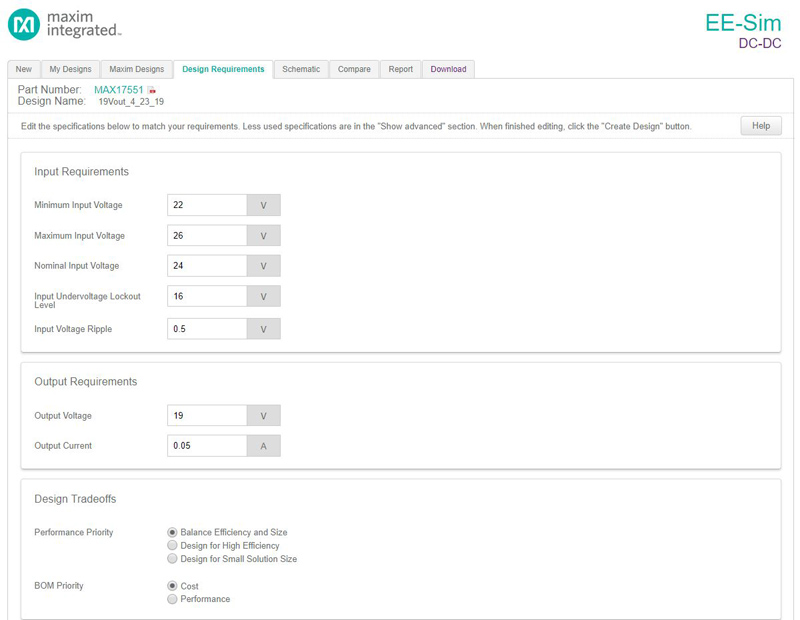
Figure 4. Input /output design requirements page in EE-Sim design and simulation tool
Looking at the op-amp diagram in Figure 2, the following op-amp equation can be used:

Where (R2||R3) =
Use Vref = 0.8V, the internal reference on the synchronous buck, and select a value for R1. In this case 261kΩ was chosen because it is on the evaluation board for the MAX17551, the synchronous buck used in this example. Some algebra can be used to solve for m and b:

yielding R3 = 46.08K and R2 = 14.63K.
Selecting the closest standard 1% values gives R3 = 46.4K and R2 = 14.7K. These standard values should be plugged back into the op-amp equation to make sure that there is still enough headroom on both the low end and high end of the DAC output.
A Variable Buck Resistor Calculator, available for download from the Power and Battery Management section of this product design calculator page, can make this task easier.
Simulate the Design at the Extremes
To complete the circuit design, we utilized a tool based on SIMPLIS that can be used to design a power supply, modify the design, and check the results. Begin the design by going to the EE-Sim webpage,selecting the MAX17551, and entering in the desired input and output values. This example used a nominal 24V supply and a 19V output voltage. The highest output voltage (19V) was selected so that the online tool will select the proper values for L1 and C1 (Figure 1). C1 is critical to stability and, since the true capacitance decreases with higher bias voltages, it is best to start the design with the highest output voltage value expected. Later, the feedback resistor will be changed for the lowest expected output voltage. In this way, the design can be checked at the extremes for stability. Figure 4 shows the design requirements screen for the design tool.
Click image to enlarge
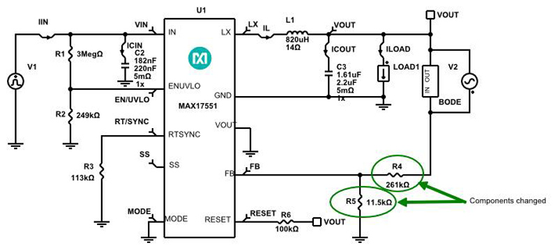
Figure 5. Schematic generated by EE-Sim design and simulation tool
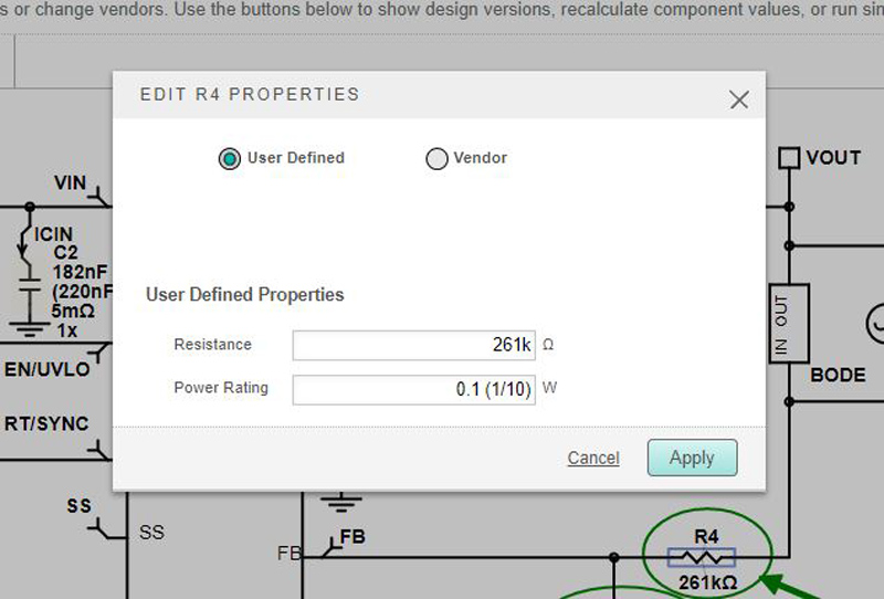
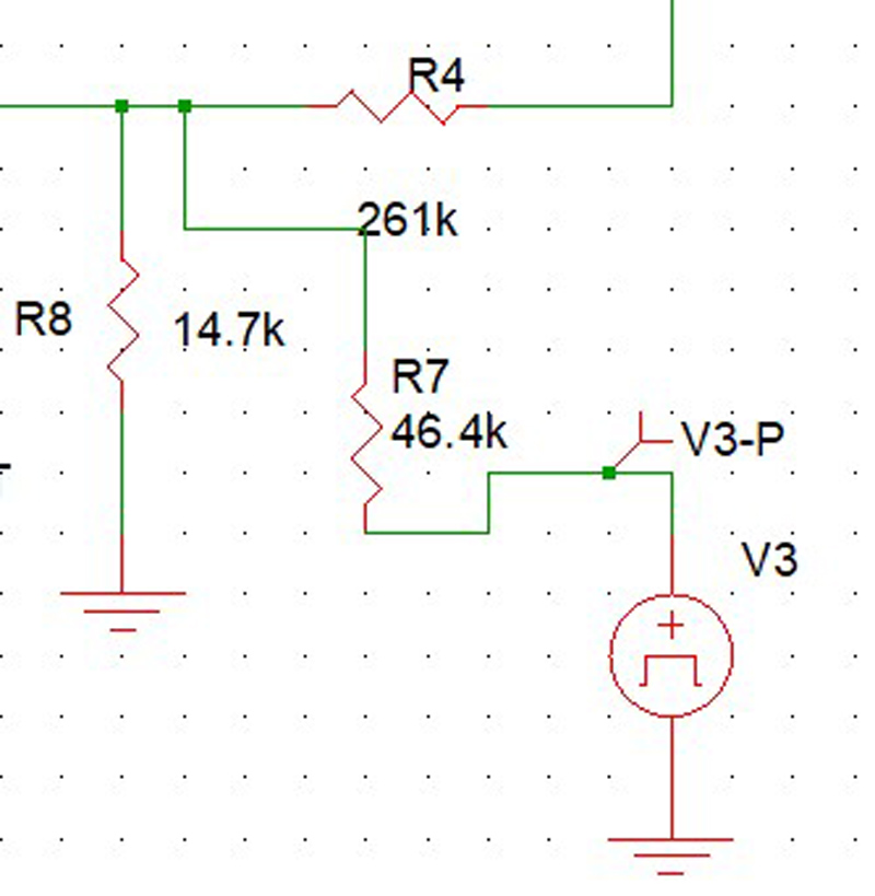
Once the design tool has generated the circuit, the components can be changed by double-clicking on the component. For instance, if you have a favorite inductor vendor, double-click on inductor L1. From there you can select from one of the many prepopulated inductors, or you can enter in user-defined inductor values. Note that if you change one of the critical values, such as L1, C2, or C3 (Figure 5), the design may require recalculation. For this example, only the feedback resistors were changed, and they are not critical to the loop compensation.
Click image to enlarge
Figure 6. Entering a user-defined value
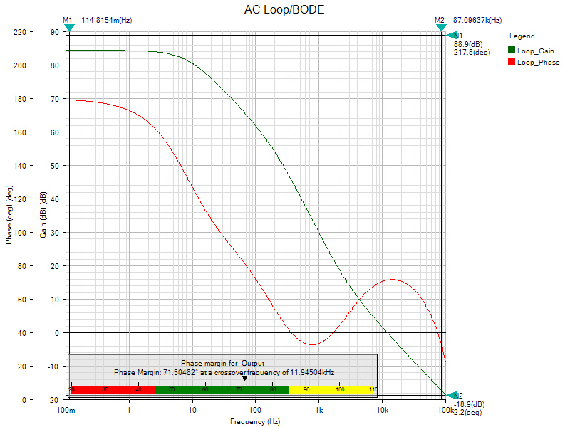
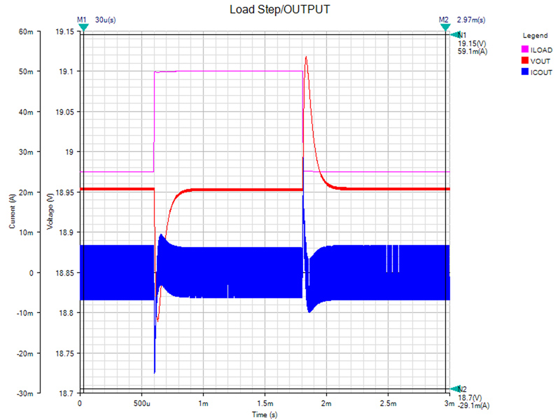
R4 was changed to 261K to match the evaluation kit and R5 was changed to maintain the 19V output. The simulations for AC analysis and a 50mA load step were run on the design and the results are shown in Figures 7 and 8. Note that there is 71⁰ of phase margin at the crossover frequency and the load step shows an excursion of about 150mV.
Click image to enlarge
Figure 7. 19Vout Bode plot generated by EE-Sim
Click image to enlarge
Figure 8. 19Vout load step generated by EE-Sim
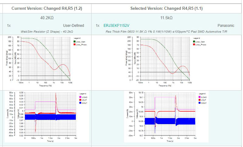
Once the highest output voltage portion of the design has been entered and verified, the lower resistor in the feedback path (R2 in Figure 1) should be changed for the lowest output voltage. Name and save the design in EE-Sim and change R5 to a value that will give an output for the lowest voltage (in the example, R5 is replaced by a 40.2K resistor for a 6V output). Re-run the simulations to make sure that it converges and has phase margin and good step response. EE-Sim allows you to compare old versus new designs, and this makes for a quick and easy way to check the changes that have been made.
Click image to enlarge
Figure 9. Comparison of 19V and 6V designs
The phase margin of the 6V design is now 62⁰ as we might expect, since the “amplifier” is now operating at a “lower gain.” The crossover frequency has moved from 12KHz at 19Vout to 37KHz at 6Vout. Still, there’s plenty of phase margin and the load step looks fine.
Offline Simulation Engine
Now that the design has been checked out via simulation, the 19V design that was saved can be downloaded and run offline on an offline simulation engine. This example used the EE-Sim OASIS Simulation Tool, which allows you to change the design or add components that are not available in the online design tool. For this example, the three resistor values calculated earlier were added and a waveform generator was added in place of the DAC. The waveform generator can be set up for a variety of waveforms (square, sine, sawtooth, etc.) and has some other features that enable it to work with the simulator. Delaying the start-up and idling the waveform generator during POP analysis helped.
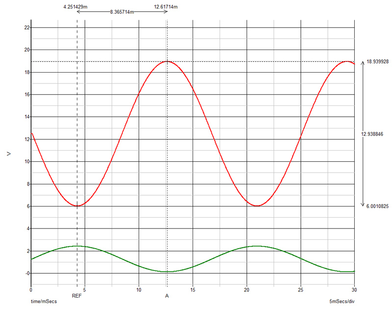
For this example, a 60Hz sinewave was chosen to drive the 0.1V to 2.4V input in simulation. The sinewave shows off the versatility of both the synchronous buck and the offline simulation tool (besides, it might be useful to have a 60Hz “power” sinewave). Figure 10 provides the section of the schematic that was modified and Figure 11 shows the time domain (transient) results for both the input and the output.
Click image to enlarge
Figure 10. Feedback resistor changes and waveform generator
Click image to enlarge
Figure 11. Transient response from OASIS Simulation Tool
The simulations show that the design behaves as expected, generating a 13V sine wave that varies between 6V and 19V when stimulated by a 0.1V to 2.4V signal. The design file for the MAX17551 variable buck regulatoris available for download.
Measured Results
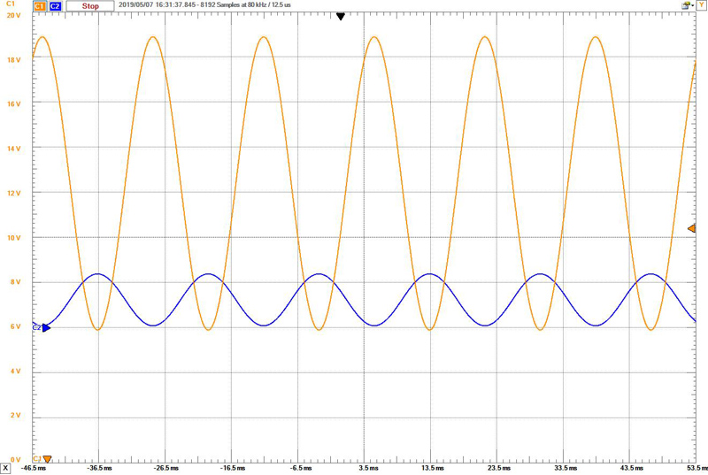
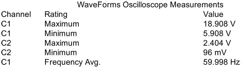
The design and simulation tool generates a bill of material (BOM) and makes it easy to purchase the parts required to build up a prototype board. In this case, the evaluation kit for the MAX17551 was modified with the components generated. A 0.1 to 2.4V sine wave was injected into the summing node and a 400ohm load was added. The results are shown in Figures 12 and 13, and they closely match the simulated results.
Click image to enlarge
Figure 12. Oscilloscope capture from modified evaluation kit for the MAX17551
Click image to enlarge
Figure 13. Measurement readings from modified evaluation kit
Summary
Variable output buck converters can be useful for many applications, but it is important to choose the right converter that can cover the range of voltages and then check the design for stability at the output extremes. Modern simulation tools can greatly speed up the design process and improve the chances for a successful design.
Maxim Integrated