How to Improve Thermal Performance of Ignition IGBTs
Higher rates of environmental pollution and demanding government vehicle efficiency regulations are driving new technology investments in transportation
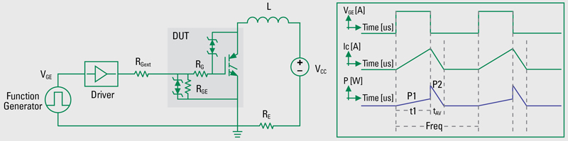
Figure 1. Simplified schematic of the Ignition IGBT test circuit and the resulting IGBT gate voltage, collector current, and dissipated power. P1 is the ON-state power loss and P2 is the discharging cycle power loss
As a result of greater pollution and more stringent regulations, electric and hybrid research and development includes developments in more efficient internal combustion engines and alternative fuels. While the all-electric vehicle is considered the leading solution to eliminate pollutants from vehicles, a number of factors are slowing their mass adoption. At the present time, both electric vehicles and hybrid electric vehicles are more expensive than traditional vehicles, comparable internal combustion-based vehicles and electric vehicles have distance limitations due to battery capacity. Re-charging the battery can cause a significant delay in a trip due to the number of hours required to re-charge. Furthermore, the most significant impediment is the lack of charging infrastructure compared with the ubiquitous gas station.
As a result of the current challenges with electric vehicle technology, the internal combustion engine is a long way from becoming an obsolete technology. Manufacturers are responding to lower government greenhouse gas emission limits and higher mileage standards by creating internal combustion engines and hybrid engines that are smaller in volume, operate at higher revolutions/minute (RPMs), and work with leaner fuel mixtures.
Smaller engine volume could require development of smaller cylinders. To maintain an appropriate output power, higher combustion cycle rates are needed. The ignition system will be required to operate at higher switching frequencies and be subjected to higher operating temperatures.
Diluted mixtures at low- and mid-load will require the use of wider spark gaps to ensure sufficient heat transfer when the combustion process is initiated. The use of wider gaps requires higher ignition circuit voltage ratings to initiate the arc in the spark gap.
Alternatively, a direct injection process during the compression stroke avoids the mixture homogenization and forms a fuel rich zone in the proximity of the spark while keeping the total mixture lean. This achieves an additional efficiency improvement. The fuel spray must generate favorable conditions for the combustion development at the time and location of the spark. However, the high local and temporal variation close to the spark compromise the ignition system, that ideally should contain a wide ignition space (larger electrode gap) and a longer ignition time. These conditions would require a higher breakdown voltage and greater energy in the spark.
These innovations will have a significant impact on the engine’s solid-state ignition system. The primary power control element of the ignition system, an ignition insulated gate bipolar transistor (IGBT) will have to support higher energy to achieve new engine efficiency levels. The ignition IGBTs also will require higher clamping voltages to ignite leaner fuel mixtures and will operate at higher frequencies to generate more power in smaller engines. These operating conditions will increase the IGBT’s thermal dissipation. Under these conditions, the IGBT’s collector -to-emitter ON-state voltage (Vce(ON)), which is directly correlated to the ON-state power losses, will gain greater significance. Ignition IGBTs with lower Vce(ON) will be required to reduce power losses and, consequently, achieve lower junction temperatures, while maintaining a small system footprint.
The challenge for the designer is both selection of an appropriate IGBT and use of good technique in printed circuit board (PCB) layout. The designer must select an IGBT with adequate power handling capacity and low switching power loss. That entails selecting an ignition IGBT with low Vce(ON) to minimize ON-state power consumption. The designer must also use optimal PCB pads both to dissipate the additional heat created by the higher power state of the ignition IGBT and to maintain a controlled thermal junction temperature within the device’s specifications.
To aid the design engineer, Littelfuse, a manufacturer of circuit protection, sensing, and power control products, has provided quantitative data (presented below) to show how an IGBT with a lower Vce(ON) and how different thermal PCB pad constructions affect the thermal performance of ignition IGBTs. A Littelfuse ignition IGBT housed in a TO-252 (also known as DPAK) surface mount package for high power components and another manufacturer’s device are used in the study.
All test data was obtained using the simplified diagram of the test bench setup shown in Figure 1. A load inductance of 0.3 mH was used in order to emulate a common value of the leakage inductance of commercially available Ignition coils. The switching frequency is set to either 33 Hz, 50 Hz, 80 Hz, 100 Hz or 150 Hz. The dwell time, or time that the Ignition IGBT is in the ON-state, is set to achieve 10 amps of peak current. The Device Under Test (DUT) is then placed in one of the different PCB PADs shown in Figure 2 and left operating for 10 minutes, ensuring a steady state temperature measurement.
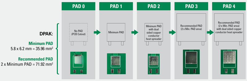
Five types of PADs were analyzed to study the effect of different thermal conduction paths on IGBT case temperature (Figure 2). The pad types were:
· a PCB cutout (PAD 0) where there is no heat conduction path from the collector of the Ignition IGBT to the PCB,
· a PAD with the same area as a DPAK packaged IGBT (PAD 1),
· a PAD with the same area as a DPAK packaged IGBT but including heat spreaders from the top to the bottom of the PCB (PAD 2),
· a PAD with the recommended PAD area for a DPAK packaged device (twice the area of the device) without thermal heat spreaders from the top to the bottom of the PCB (PAD 3), and
· a layout identical to PAD 3 with thermal heat spreaders from the top to the bottom of the PCB (PAD 4).
Click image to enlarge
Figure 2. The PCB pad layouts used for the thermal analysis
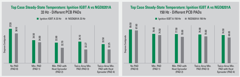
Figure 3 quantifies the effect of a lower Vce(ON) on the thermal performance. The Ignition IGBTs used in the comparison are Littelfuse DPAK packaged NGD8201A (Vce(ON)typ<1.35V), and a commercially available Ignition IGBT (Vce(ON)typ<1.5V) labeled as “Ignition IGBT A”. These devices were chosen since they possess similar electric and physical die characteristics and equivalent current and energy ratings. Figure 3 summarizes the measured steady state case temperatures achieved for each of the different PCB PAD layouts when driving the Ignition IGBT at frequencies of 33 Hz and 150 Hz. The slightly higher ON-state voltage of “Ignition IGBT A” results in a slightly higher steady state temperature, regardless of the PCB PAD used. As expected, this effect is more noticeable at high switching frequencies. Notice also that the use of different PCB PADs results in different steady state case temperatures.
Click image to enlarge
Figure 3. Comparison of the steady-state temperature of two Ignition IGBTs operating at 33Hz and at 150Hz. The NGD8201A Ignition IGBT has a lower Vce(ON) that results in a lower steady-state temperatures for all PAD configurations
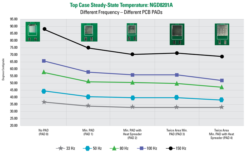
The effect of the use of the different PCB PADs can be further analyzed in Figure 4, where the steady state case temperature for the NGD8201A is shown when different switching temperatures and PADs are considered. Once more, the results show that the use of a higher switching frequency results in higher steady state temperatures. However, of special importance is the effect of the PAD on reducing the measured temperature, especially when working at high switching frequencies. For instance, notice how the steady state temperature, when working at 150 Hz, is reduced from ~90 °C to ~70 °C when the minimum PAD with heat spreaders between top and bottom layer (PAD 2) or a PAD with the recommended area (twice the area of a DPAK, PAD 3) are used.
Click image to enlarge
Figure 4. NGD8201A top case steady state temperatures obtained for switching frequencies using the five PCB PAD layouts
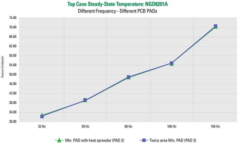
For a better comparison, the obtained steady state case temperature under different frequencies are plotted when using the minimum PAD with heat spreaders between top and bottom of the PCB (PAD 2) and the recommended PAD of twice the area of a DPAK (PAD 3). It is shown that regardless of the switching condition, these two PADs can offer the same averaged thermal dissipation capability. This is of special importance in Ignition platforms in which size needs to be considered.
Click image to enlarge
Figure 5. Steady-state case temperature of the NGD8201A operating from 33 Hz to 150 Hz using (PAD 2) and PAD 3 layout configurations. The results are nearly identical
The automotive industry is designing more fuel-efficient internal combustion engines to meet the challenges demanded by more strict government regulations on lower fuel consumption and reduced CO2 emissions. The new engine enhancements will require ignition systems that can sustain higher energy and higher voltage to ignite leaner fuel mixtures. Ignition IGBTs will need to be capable of supporting higher energy with higher switching frequencies and higher voltage for spark initiation. As a result, the IGBTs will be subjected to higher operating temperatures. Selecting an IGBT with lower Vce(ON) and using an appropriate PCB pad layout that provides good thermal dissipation can ensure reliable operation in the harsh environment of an internal combustion engine.


