How to Increase High-Power EV Battery Charging using Surface Mount Power Devices
To achieve broader consumer acceptance of electric vehicles (EVs), today's designers must solve the fast-charging challenge
End users expect new EV designs to minimize vehicle idle time, especially for long-distance driving. EV automotive designers need to increase charger power output, power density, and efficiency to achieve the fast-charging end-users expect. Single-unit, charger designs currently range from 7 kW to 30 kW. The combination of single-unit assemblies into modular designs increases power output, helping charger manufacturers to achieve their goals regarding smaller footprint, higher flexibility, and scalability. Using advanced isolated packaging for the active power components addresses the high-power charging challenges by enabling even higher power density and significantly reducing the efforts in thermal management in circuit designs.
Electric utilities have the additional challenge of managing the large loads resulting from the increasing EV usage from charging EV batteries. Utilities are investigating two vehicle-to-grid technologies:
· V1G – In this technology, known as smart charging, the utilities individually distribute the energy to minimize demand peaks in two ways; by controlling the time when charging an EV starts, and the magnitude of power supplied.
· V2G – Bi-directional charging controls the charging time, power, and direction. For example, to reduce peak demand, the utility could pull some power from a fully charged battery back to the power grid to supply it to another vehicle.
The V2G approach can be very cost-efficient for vehicle fleets, as contributing to peak-shaving would be considered a valuable service. Case in point, most school buses run only during the day and are available for charging and sharing power all night. A more extensive fleet, like the 500,000 school buses operated in the United States, could be controlled as highly decentralized energy storage. The available battery capacity can grow to a regime of GWh during the 100 days of US summer vacation idle time. To accommodate the V2G technology, today's designers need to develop bi-directional chargers that can also supply energy to the power grid.
Compared to the simpler uni-directional chargers, the bi-directional designs are more complex, requiring more components. Additional effort is also needed to manage power dissipation and develop sophisticated control algorithms.
Handling higher power requires advanced packaging of high-power semiconductors
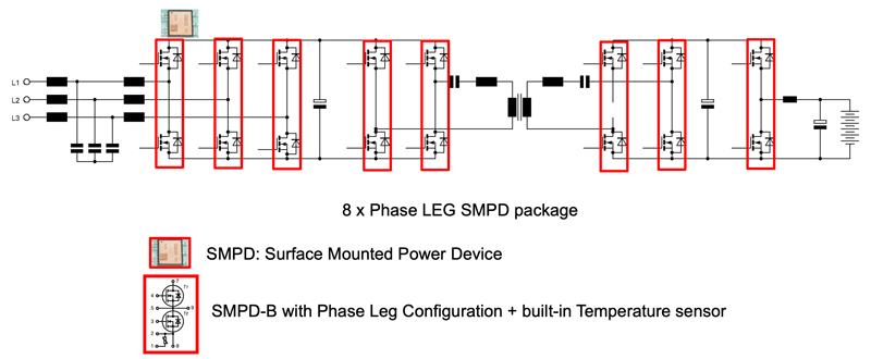
A bi-directional power supply topology employing 16 SiC power MOSFETs in sets of eight half-bridges is shown in Figure 1. To achieve higher power, electronics designers can utilize more discrete power FETs in parallel; however, this complicates the design of the power-electronic system. The discrete power FET packaging is usually a D²PAK or a TO-247 package. When designing for power levels exceeding 30 kW, advanced isolated packaging provides components that support the required high output power.
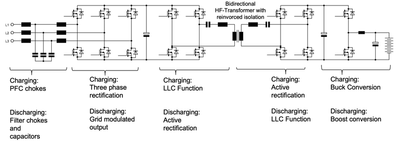
Click image to enlarge
Figure 1: Bi-directional charger circuit with multiple power conversion stages
In contrast to discrete packages, isolated packages allow the mounting of multiple packages onto a common heatsink. Because of their low profile, they offer a more compact design by minimizing the overall height of the subunit compared to their 12- or 17-mm power-module counterparts. Furthermore, using a top-cooling side featuring high insulation strength, there is no need for additional isolation foil between the device and heatsink, making the assembly process easier and less costly.
An example of the packaging options and their power handling capability is given in Figure 2. These packaging options are rated by the output power and thermal dissipation as well as the printed circuit board (PCB) layout complexity and assembly difficulty. The surface-mounted power device (SMPD) provides the designer with the best combination of power capability, power dissipation, and ease of layout and assembly.
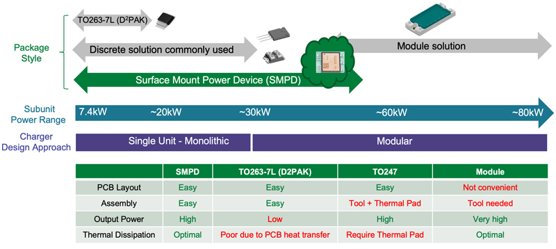
Click image to enlarge
Figure 2. Packaging power capability with comparison of packaging performance
SMPD Packaging Implementation for Higher Power Density
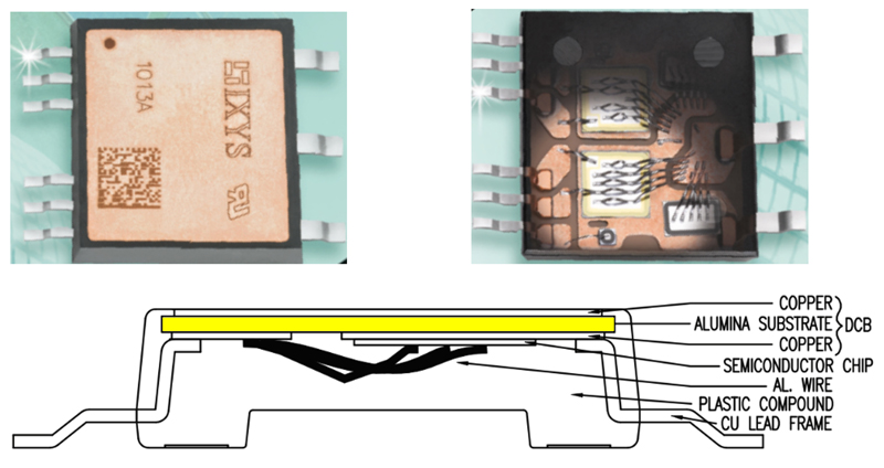
EV charging system designers can use SMPDs to house various chip-technologies, incorporating various voltage classes and circuit topologies, including half-bridges. An example of the SMPD packaging is depicted in Figure 3. The SMPD package features:
· Direct Copper Bonded (DCB) substrate with a copper lead frame,
· aluminum bond wires, and
· a plastic molding compound around the semiconductor.
The DCB structure offers high isolation strength, thus enabling a multi-semiconductor arrangement with high thermal dissipation capabilities on a single carrier. The DCB's exposed copper layer maximizes the available surface area for a heat sink connection. A copper lead frame combined with aluminum bond wires makes simplified soldering and assembly possible.
Click image to enlarge
Figure 3. Example Surface-Mount Power Device (SMPD) package (Source: Littelfuse)
The design of the SMPD package in this example offers several advantages:
· UL-recognized, insulation voltage rating up to 2500 V
· Lower thermal resistance compared to other semiconductor packaging like TO-style devices.
· SMPD provides a higher current carrying capacity than available with TO-style packages.
· Reduced radiated EMI due to low parasitic coupling capacitance between the semiconductor die and the heatsink.
· Maximized utilization of the semiconductor's capabilities and low voltage-overshoot result from the package's low stray inductance.
· There is greater flexibility in enabling customized topologies, including thyristors, power diodes, MOSFETs, and IGBTs.
· Because of the isolated backside, all power semiconductors can mount onto a single heat sink.
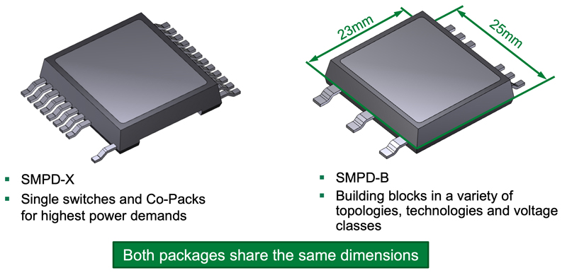
As Figure 4 illustrates, the SMPD package is available in two versions, SMPD-X and SMPD-B. The SMPD-X contains a single switch, single diode, or Co-Pack to cover higher power demand in one package. The SMPD-B allows building blocks in a wide variety of voltages, currents, and technologies such as MOSFETs, IGBTs and thyristors in a variety of topologies.
Click image to enlarge
Figure 4: SMPD-X and SMPD-B package comparison
Both versions have the same package dimensions of 25 mm length and 23 mm width and share a common footprint and mounting area.
A 19-inch rack, built with two Height-Units (2HU) and a length of 880 mm for EV charging subunits is ubiquitous in the industry. When using low-profile SMPD packages, as an example, the design exhibit roughly a 13 percent volume saving compared to E2, and E3 Package in a 19-inch 2HU rack configuration, resulting in more space for passive components such as power magnetics and decoupling capacitors.
SMPD packaging reduces the number of components by almost 50%, as illustrated in Figure 5. Reducing the number of components required allows for enhanced power density, higher power, and the reduction of the overall assembly size. Each package shown in Figure 5 contains two power MOSFETs as one example of multiple circuit configurations available in SMPD packaging.
Click image to enlarge
Figure 5. Bi-directional charger built on SMPD packaging reduces the component count by nearly 50%
In case even higher power levels are targeted, the SMPD is also available with single-switch arrangements for IGBT and SiC MOSFETs. Once designs demand higher voltages, package options up to and exceeding 1700 V are readily available.
The goal: Smaller packages with higher power
By incorporating SMPD packaging, designers can increase the power of their EV chargers, thus improving power density and efficiency. SMPDs enable designers to develop single power units with output as high as 50 kW without paralleling components. Using SMPD power components helps lower the manufacturing cost by using fewer components. Surface-mounted package designs like those from Littelfuse can minimize heatsink size and cost with low thermal resistance packaging technology. Using this packaging can lower both radiated and conducted EMI with lower parasitic capacitance and stray inductance. The designer can also use smaller inductors by operating at higher frequencies, further saving space and cost.
Bottom line: SMPD power device packaging helps designers overcome the challenges of increasing the output power without substantially increasing the size and weight of the system built.