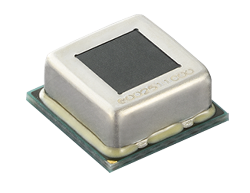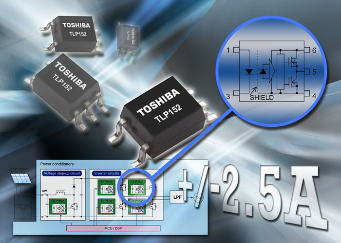
Targeting applications such as factory automation equipment, motor drives, digital home appliances, and photovoltaic power micro-inverters, the TLP152 gate drive coupler from Toshiba Electronics Europe can reduce PCB space and power consumption in IGBT and MOSFET designs that need galvanic isolation. The gate drive coupler is designed to directly drive IGBTs and power MOSFETs without the need for additional components. A miniature S06 package reduces mounting area by 50% compared to the widely used SDIP packaged devices. In addition, by lowering minimum supply voltage to 10V, the new coupler also helps to reduce power consumption. The SO6 package provides a minimum isolation voltage of 3750Vrms and is compatible with reinforced insulation requirements of international safety standards. Guaranteed minimum creepage and clearance distances are 5mm and internal insulation thickness is 0.4mm. An internal noise shield provides a guaranteed minimum common mode transient immunity of +/-20kV/?s. The TLP152 is compatible with a wide 10V to 30V input range that minimizes the need for additional power conversion circuitry. Maximum supply current is 3mA. A buffer logic type totem pole output can deliver a maximum peak output current of +/-2.5A Designed for high-speed operation, the TLP152 has a maximum propagation delay of 200ns. Construction is based around a GaAlAs infrared LED optically coupled to an integrated high-gain, high-speed photodetector IC. The S06 package has dimensions of 7.0mm x 3.7mm x 2.1mm and the guaranteed operation temperature ranges from -40° to 100°C.