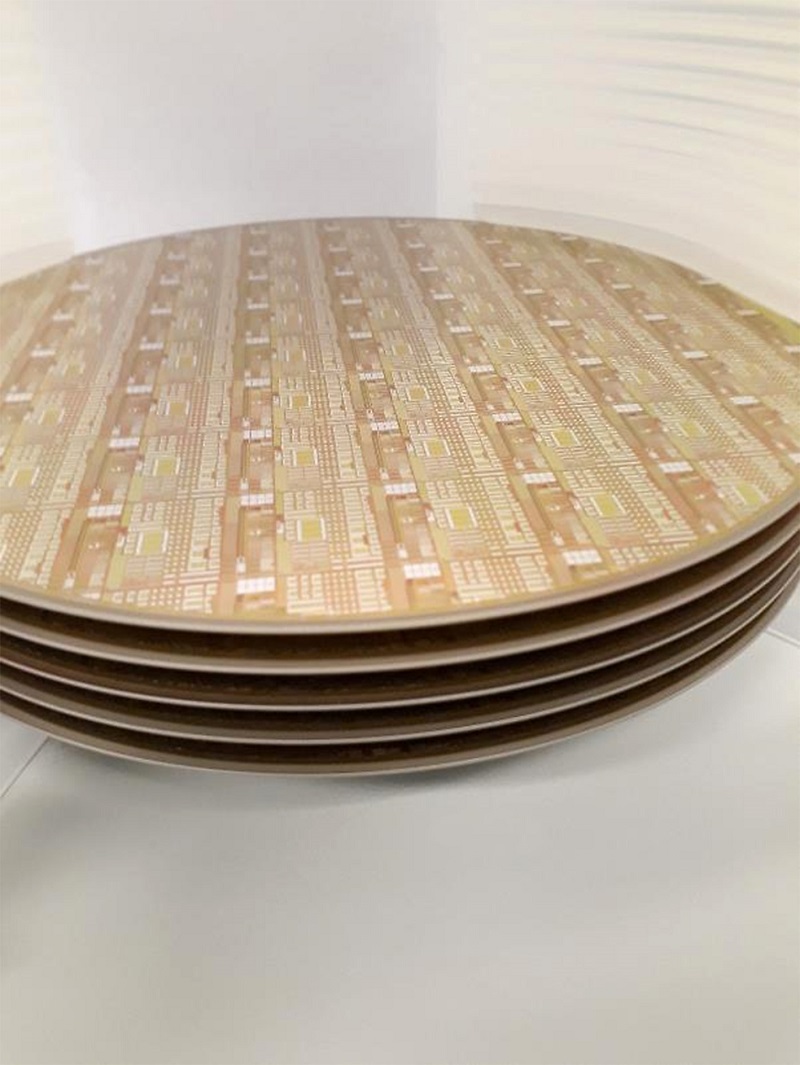
Imec and Qromis Present High Performance p-GaN HEMTs on 200mm CTE-matched Substrates
imec and Qromis, have announced the development of high performance enhancement mode p-GaN power devices on 200mm engineered Coefficient of Thermal Expansion (CTE)-matched substrates, processed in imec’s silicon pilot line. The substrates are offered by Qromis as commercial 200mm QST® substrates as part of their patented product portfolio. The results will be presented at next week’s CS international Conference (April 10-11, Brussels, Belgium).
Today, GaN-on-Si technology is the industry standard platform for commercial GaN power switching devices for wafer diameters up to 150mm/6 inch. Imec has pioneered the development of GaN-on-Si power technology for 200mm/8 inch wafers and qualified enhancement mode HEMT and Schottky diode power devices for 100V, 200V and 650V operating voltage ranges, paving the way to high volume manufacturing applications. However, for applications beyond 650V such as electric cars and renewable energy, it has become difficult to further increase the buffer thickness on 200mm wafers to the levels required for higher breakdown and low leakage levels, because of the mismatch in coefficient of thermal expansion (CTE) between the GaN/AlGaN epitaxial layers and the silicon substrate. One can envisage to use thicker Si substrates to keep wafer warp and bow under control for 900V and 1200V applications, but practice has learned that for these higher voltage ranges, the mechanical strength is a concern in high volume manufacturing, and the ever thicker wafers can cause compatibility issues in wafer handling in some processing tools.
Carefully engineered and CMOS fab-friendly QST® substrates with a CTE-matched core having a thermal expansion that very closely matches the thermal expansion of the GaN/AlGaN epitaxial layers, are paving the way to 900V-1200V buffers and beyond, on a standard semi-spec thickness 200mm substrate. Moreover, QST® substrates open perspectives for very thick GaN buffers, including realization of free-standing and very low dislocation density GaN substrates by >100 micron thick fast-growth epitaxial layers. These unique features will enable long awaited commercial vertical GaN power switches and rectifiers suitable for high voltage and high current applications presently dominated by Si IGBTs and SiC power FETs and diodes.
“QST® is revolutionizing GaN technologies and businesses for 200mm and 300mm platforms”, stated Cem Basceri, President and CEO of Qromis. “I am very pleased to see the successful demonstration of high performance GaN power devices by stacking leading edge technologies from Qromis, imec and AIXTRON,” Basceri said.
In this specific collaboration, imec and Qromis developed enhancement mode p-GaN power device specific GaN epitaxial layers on 200mm QST® substrates, with buffers grown in AIXTRON’s G5+ C 200mm high volume manufacturing MOCVD system.
Imec then ported its p-GaN enhancement mode power device technology to the 200mm GaN-on- QST® substrates in their silicon pilotline and demonstrated high performance power devices with threshold voltage of 2.8 Volt. “The engineered QST® substrates from Qromis facilitated a seamless porting of our process of reference from thick GaN-on-Si substrates to standard thickness GaN-on- QST® substrates using the AIX G5+ C system, in a joint effort of imec, Qromis and AIXTRON,” stated Stefaan Decoutere, program director for GaN power technology at imec. The careful selection of the material for the core of the substrates, and the development of the light-blocking wrapping layers resulted in fab-compatible standard thickness substrates and first-time-right processing of the power devices.
Imec acknowledges funding from the Electronic Component Systems for European Leadership Joint Undertaking under grant agreement No 662133, designated as PowerBase.
www.imec.com


