Imec reveals impact of DSA process variations on electrical performance of DSA-formed vias
Leading nanoelectronics research center imec presenedt electrical results of DSA (directed self-assembly)-formed vias, gaining insight in the impact of DSA processing variations on electrical readout, at the SPIE Advanced Lithography Conference (San Jose, Feb 21-25). DSA processes with cylinder-forming block copolymers (BCP) have gained attention for contact hole shrink applications with improved contact hole roughness, and for their potential to increase the contact hole density that is obtained with optical lithography.
R&D efforts have focused on optimizing the process to obtain (pre-pattern) templates resulting in straight profiles after the DSA process, on increasing the feature density and on maximizing the open hole yield after pattern transfer. However, knowledge on electrical results from such DSA-based shrink processes is scarce.
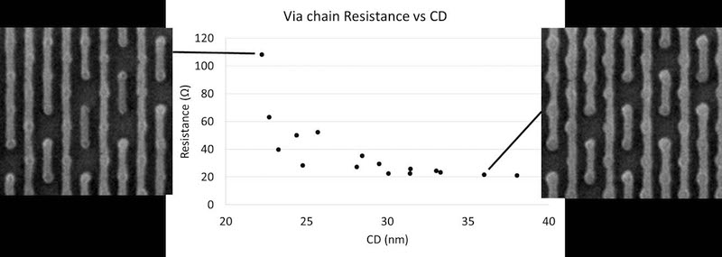
Over recent years, imec has developed a templated grapho-epitaxy DSA flow for contact hole shrink and multiplication. Imec has applied this DSA flow to a short-loop test vehicle based on its 28nm node technology. Through testing the electrical performance of the DSA-formed vias, imec determined the via chain resistance as a function of process conditions including template dimension and BCP film thickness. Among a set of process conditions, increasing via chain resistance is observed with decreasing via CD (critical dimension). SEM images indicate high-quality via filling after metallization. The learning is now being applied to DSA via patterning in imec’s N7 technology.
Imec’s research into advanced patterning is performed in cooperation with imec’s core and strategic IC manufacturing partners including Samsung, Micron, Intel, Toshiba-Sandisk, SK Hynix, TSMC, GlobalFoundries and material and equipment makers.