Author:
Anup Bhalla, V.P. Engineering at UnitedSiC
Date
01/05/2021
 PDF
PDF
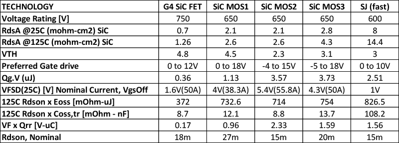
Table 1: Comparison of parameters for G4 750V SiC FETs with similar 650V SiC MOSFETs and 600V Superjunction fast diode FETs
The automotive market for Silicon Carbide (SiC) devices is widely expected to exceed the $1.5 billion threshold in 2025 with an annual growth rate (CAGR) of 38 percent. This is driven by the value provided by SiC based components in On-board chargers, DC-DC converters and in Traction inverters. With the launch of its 750V generation 4 (G4) SiC FET technology, UnitedSiC provides designers with devices that can improve power density, reduce power losses, and improve cost-performance metrics for new designs.
Gen 4 Technology
The ideal power semiconductor switch would have negligible losses in the on-state, during turn-on and turn-off transients, be easy to drive, safely block high voltages and be robust against over-voltage and short-circuit events. SiC based switches bring high voltage >650V devices closer to this goal. With the evolution of technology, power semiconductor vendors can handle the same power conversion task with smaller devices, by reducing both conduction and switching losses, while maintaining sufficiently good thermal capability and robustness. This helps to progressively improve power density with more compact power converters and inverters, at increasingly attractive prices. Silicon devices such as Superjunction FETs and IGBTs continue to evolve but the pace of improvement in wide band-gap devices, particularly SiC FETs has been much more rapid, since SiC is earlier in its cycle of technological maturity.
Table 1 shows a comparison of key parameters and figures of merit for UnitedSiC Gen 4 SiC FETs (UJ4C075018K4S 18mohm, 750V) vs 650V SiC MOSFETs and Si SJ FETs. Despite the 100-150V higher voltage rating, the on-resistance per unit area of this SiC technology and 25C or 125C is 2-3X better than 650V SiC MOSFETs and >10X better than Si Superjunction devices. This is a direct result of the high-density trench SiC JFET structure within the SiC FET, which is connected in a cascode connection with a low voltage Silicon MOSFET within the package. The small chip area of the SiC JFET for a target Rds(on) means that a very low on-resistance can be provided in a given footprint, or a smaller FET with lower capacitance can be had for the same on-resistance.
The Silicon MOSFET provides a +/-20V VGS(MAX) rating, a 5V Vth, and allows for an easy 0 to 12V gate drive. The gate drive loss can be quantified as Qg.V, and this is much lower than for other SiC or Si technologies, allowing devices to be switched 3-10X faster in soft-switched circuit without overheating the existing gate drive ICs.
The body diode of the SiC FET provides a combination of low forward drop VFSD, and low QRR, which is captured in the unmatched VF.QRR figure of merit for these devices. The devices remain simple to parallel in this mode and can be used both with and without synchronous rectification.
Device capacitances for a given Rds(on) are low, driven by the small chip size, and this leads to excellent hard and soft switching figures of merit RDS*EOSS and RDS*COSS(TR) , both of which relate to the output capacitance behavior of the G4 SiC FETs. Given the fact that this device can be driven even with 0 to 10V like Superjunction MOSFETs, they provide a much simpler path to much higher frequency switching, especially in LLC circuits.
In order to deal with the thermal resistance implications of small die size, the 3X better thermal conductivity of SiC over Si is a start, but not enough. UnitedSiC also thins the SiC die to reduce electrical and thermal resistance and attaches it to the Copper lead frame in discrete packages using Ag sintering material that has 6x better thermal conductivity than standard solders. With these improvements, excellent junction-case thermal resistance RthJC numbers can be obtained.
SiC FETs with sub 10mohm on-resistances in standard TO packages have been available from UnitedSiC for demanding applications. Table 2 compares the behavior of the G3 7m, 650V device with that of a G4 6m, 750V device, both in the same TO247-4L package, which includes about 1mohm of package resistance. The RdsA of the G4 technology is half that of the G3, and this leads to a relative die size reduction of 0.65:1. The lower capacitances result in lower QRR and lower Switching loss ETOT (EON+EOFF). The impact of the smaller die is to increase thermal resistance from 0.15C/W to 0.21C/W. G4 devices have a higher rate of increase of Rds(on) with temperature, which should be factored into device choice based on estimated operating temperatures and the split between conduction and switching losses. Finally, G4 devices designed for inverter use feature excellent short circuit capability, which simplifies the protection of these devices using standard IGBT drivers and de-sat circuitry.

Click image to enlarge
Table 2: Comparison of Gen 3 650V and Gen 4 750V SiC FETs from UnitedSiC
G4 SiC FETs in On-board chargers and DC-DC converters
The 750V rating of the G4 SiC FETs allows them to be used for higher battery voltages (up to 500V) than 650V devices while preserving sufficient voltage margin, so that users need not compromise performance and cost by using 900V/1200V devices in those instances. Even with the extremely fast switching speed of these devices, UnitedSiC offers guidelines on using surface mount snubber components to manage voltage overshoots, while simultaneously maximizing the low on-resistance, low switching loss benefit of these devices in practical designs.
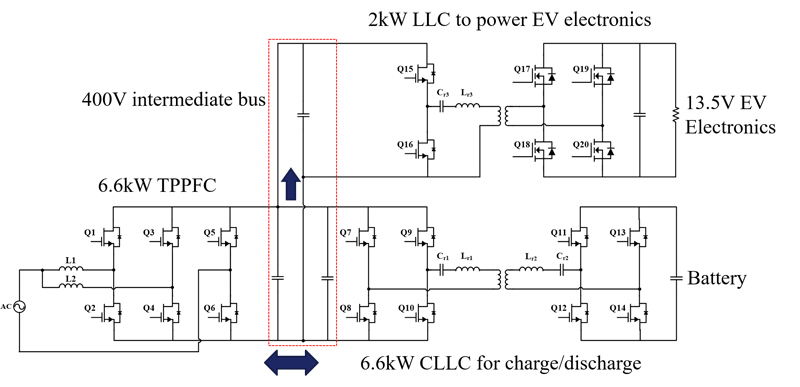
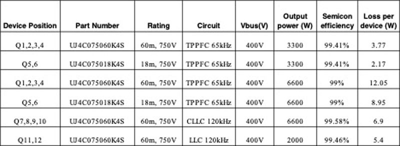
Figure 1 shows a typical circuit architecture used to create a single compact unit featuring a 6.6KW class bi-directional on-board charger (OBC) and 2-3KW DC-DC converter that provides power to the 12V sub-systems in the BEV. During charging, power flows from the grid via a Totem-Pole PFC circuit to form the high voltage DC-bus (shown here to be 400V but could be 500V). The second stage is a full-bridge CLLC unit that provides resonant DC-DC conversion to charge the battery. Note that this circuit already provides for a complete reversal of power flow such that the battery can be used to send power back to the grid. SiC FET users have the additional freedom to use the devices Q11-14 as non-synchronous rectifier diodes at high frequency making control simpler and use them as LLC controlled switches when power flow is reversed. 750V G4 devices are ideally suited to the Totem-pole PFC unit as well as the primary side of the LLC/CLLC unit. Depending on the battery voltage, Q11-14 may be 750V or 1200V SiC FETs.
Click image to enlarge
Figure 1: A typical circuit architecture for a 6.6KW on-board charger and a DC-DC converter in a compact single unit with shared cooling. 750V SiC FETs are well suited for Q1-6, Q7-10 and Q15-16. Depending on battery voltage Q11-14 may use 750V or 1200V SiC FETs
Table 3 that calculates power losses in charging mode, and full load losses for the DC-DC converter for a 6.6KW system with 2KW DC-DC stage, corresponding to the circuit if Figure 1. Using G4 SiC FET devices allows the front-end PFC stage to operate at much higher frequencies than IGBT based designs, typically going from 10-20kHz to 40-100kHz. The key to the improved losses is the low switching loss and QRR of these devices for a given conduction loss level. The DC-DC stage can be operated at much higher frequencies as well, and the low Rds(on), Coss and gate drive simplicity helps make for very efficient solutions. The high efficiency naturally leads to low losses in each transistor, which in turn simplifies the thermal design of the dense on-board charger unit.
Click image to enlarge
Table 3: Power losses using G4 SiC FETs in the various switch positions of the circuit in Figure 1. The Semiconductor efficiency column is calculated from the known device conduction and switching losses and shows that the power devices alone only account for 0.4-1% efficiency loss. This translates to the low power losses per device and eases the cooling burden
Given the availability of liquid cooling in the EV on-board chargers and DC-DC converters, several options exist for packaging. Through hole devices like TO247-4L are most popular, given their wide availability and ability to dissipate large heat loads. Kelvin gate returns are important to maximize the benefit of using SiC devices, since that enables faster switching with cleaner gate waveforms. The Ag sintered low RthJC of UnitedSiC FETs is necessary in this environment to allow efficient heat removal.
Surface mount packages are also popular, with the D2PAK-3L being supplanted by the D2PAK-7L, since the latter offers a Kelvin gate return. In general, less heat can be extracted from a D2PAK-7L single device, given the much smaller Cu pad area. However, driven by the low RthJC of the sinter technology and low losses of the SiC FET devices, compact IMS (Insulated metal substrate) based solutions for such chargers and DC-DC converters are used, which has the important benefit of using all surface mount automated assembly for the many power devices.
Finally, dedicated power modules can also be employed for these applications, which are generally more costly, but have the important benefit of simplifying the power design and layout. A key area where the choice between discrete vs module solutions must be more carefully compared is when the OBC power ratings are higher, for e.g. 22KW. In this arena, more compact specialized modules will compete with more advanced integrated FET and driver solutions, as well as with power discretes devices with ever improved ratings that extend the reach of low-cost discrete solutions.
Traction inverters
The inverters needed for EV traction fall in a wide range from 60KW to over 200KW, with much higher power ratings for the range of commercial vans, buses, trucks and heavy-duty vehicles. There is a great deal of advanced engineering underway worldwide to apply SiC MOSFET and SiC FET solutions for higher power systems with higher batter voltages that need 1200V FETs. Higher voltage helps reduce RMS currents for the same power, improving system efficiency by cutting copper losses.
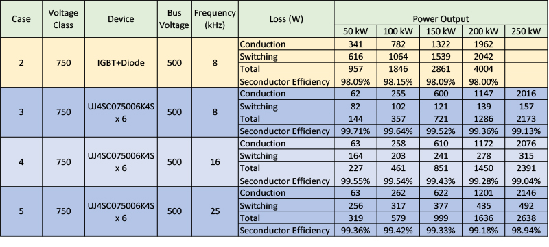
However, the highest volume designs currently in use, and the ones that will dominate personal vehicles can likely benefit from the new class of 750V G4 SiC FETs, especially as it pertains to competing with the incumbent IGBT based solution. Table 4 compares the improvement in power losses possible using the G4 SiC FETs described earlier in Table 2 relative to the best-in-class IGBT modules for this application. A 3X reduction in losses at 200KW, and a 6X reduction at 50KW ensures a stable thermal design for rapid periods of acceleration despite the much smaller chip sizes of SiC FETs, coupled with excellent range enhancement from the light load loss reduction. During regenerative breaking, IGBT based solutions have rectifier losses from the fast recovery diodes, which can be drastically reduced in SiC FETs using synchronous rectification. Given the excellent short circuit robustness of the G4 750V SiC FET and the compatibility with IGBT gate drives and de-sat protection, these devices provide an excellent upgrade path for traction inverters.
Click image to enlarge
Table 4: Comparing power losses vs output power in an IGBT based traction inverter vs one built with 750V G4 SiC FETs. A 3X reduction in full load losses and a 6X reduction is light load losses are possible, in normal traction mode, as well as in regeneration mode
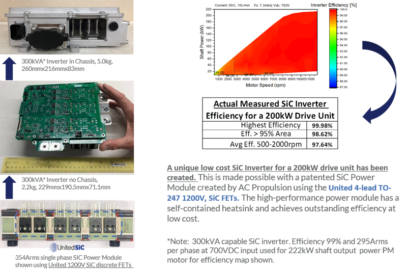
With the introduction of these ultra-low Rds(on) power discretes (sub 10mohm TO247-4L), UnitedSiC as made possible an alternative to the module-based approach to building traction inverters. Innovative designs can use the excellent paralleling capability of these devices and the ultra-low RthJC of the sintered package, to build very cost-effective high performance traction inverters. An example of such an inverter using Gen 3 technology is shown in Figure 2 (courtesy of AC Propulsion). The 300KW unit is built using 4X G3 9m, 1200V devices paralleled per switch position, and delivers very high operating efficiency across a wide load range.
Click image to enlarge
Figure 2: A 300kVA traction inverter with UF3SC120009K4S TO247-4L FETs delivers a very high performance at a low-cost point. This approach is becoming very competitive alternative to the module-based approach with the introduction of very low resistance power discretes
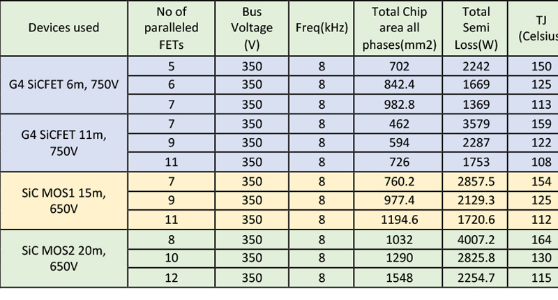
Table 5 shows a comparison of the SiC area needed to build a traction inverter using G4 750V SiC FETs vs competing SiC MOSFET technologies. In addition to the benefit in short circuit robustness, and the 100V higher rating, it is clear that the same operating junction temperature, or the same power loss point can be achieved with much less SiC area using the UnitedSiC G4 technology, driven largely by the low on-resistance per unit area of this technology.
Click image to enlarge
Table 5: Optimizing the area of SiC needed to achieve a certain loss (efficiency), output power or maximum operating temperature target is best done with SiC FETs from UnitedSiC, given their much lower RdsA. For a given area of SiC used, a much lower operating loss or temperature can be achieved. All solutions provide a much higher performance than the IGBT alternative
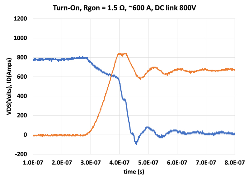
Figure 3a shows a prototype 3-phase traction inverter module based on 1200V G4 SiC FETs used as a vehicle evaluate the performance of G4 SiC FETs. The module uses 8 paralleled 9m, 1200V stack cascode G4 SiC FETs per switch position, to achieve a net on-resistance of 1.5mohm per switch at the terminals. The typical switching waveforms of this module are shown in Figure 3b. It serves to demonstrate the excellent paralleling of the chip technology as well as the efficiency benefits of migrating to SiC based designs. Module based solutions simplify system design but are generally more expensive than a discrete based solution.

Click image to enlarge
Figure 3a: A prototype six-switch module 600A, 1200V to implement a 2 level Voltage source inverter for traction applications. Each switch position uses 8 chips, each about 9mohm in resistance. Adding wire and copper resistance, each switch is 1.5mohm at the terminals
Click image to enlarge

Click image to enlarge
Figure 3b_1 & Figure 3b_2: Half-bridge switching characteristics of the 600A, 1200V 1.5mohm module with a customized gate driver board. SiC FETs offer excellent fast switching behavior, which in conjunction with the very low conduction losses, results in the very low power losses
Conclusion
These are exciting times for SiC power solutions manufacturers, where rapid technology advancements in the SiC semiconductor and packaging space have resulted in tremendous application momentum not only in EVs, but a wide range of segments. The G4 SiC FET technology described at APEC 2020, followed by worldwide product launch in Q4 2020 will likely accelerate this adoption. We expect to compete effectively with the SiC, GaN and Si offerings in this space, giving designers what they require to provide ever increasing power density and performance while meeting their demanding cost targets. In the area of traction inverters, G4 technology will provide a very compelling solution to the challenges of cost effective, highly reliable SiC based traction inverters, and can be expected to see tremendous volume growth in the coming years.