If BEVs are to be useful for long-distance journeys, the charging infrastructure has to be closer to today’s experience of refuelling a petrol or diesel vehicle.
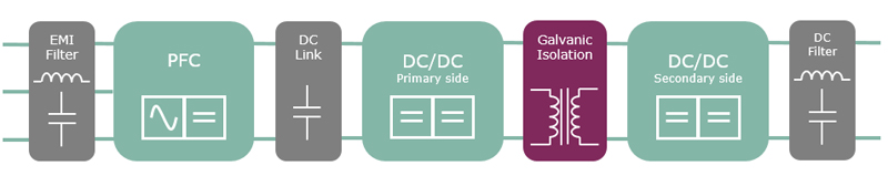
Figure 1: Typical topology for charging sub-unit in 15 – 40 kW range
One cannot fail to notice that our city streets and car parks are going through a slow transformation: they are beckoning the age of the electric vehicle. As the battery electric vehicle (BEV) grows in popularity, the infrastructure to keep them charged is appearing to meet demand. While the majority of BEVs are yet to compete on range with internal combustion engine (ICE) vehicles, range-angst need not be an issue if BEVs could be recharged in a time frame approaching that of a typical filling station visit.
For home charging, most BEVs can be charged either from the domestic AC supply or via a wall-mounted charger. Rated typically at up to 22 kW, such solutions provide enough charge for a further 200 km in around 120 minutes. This is ideal for overnight refuelling. However, to achieve the same range in around 15 minutes (one-eighth of the time) would require a DC charger rated at 150 kW. Such power can only be delivered in dedicated locations where the necessary electrical infrastructure is in place, with service stations, taxi ranks and existing filling stations being ideal candidate locations.
Taking a modular approach
Regional standards for chargers are already well established, with organisations such as CharIN in Europe, CHAdeMO in Japan, and GB/T in China having defined everything from connectors and cables to charging voltages and currents. Further standards are also applicable that cover general aspects of electrical safety (IEC 60950), optical isolation (UL1577) and magnetic and capacitive (VDE V 0844-11) coupling components. This leaves developers the freedom to choose how to best approach the implementation of the DC charger.
Issues such as form factor, environment, aesthetics and price will influence many aspects of the design. However, regardless of these requirements, DC chargers in the 50 kW to 150 kW range will require a modular approach. These are linked together via a data bus to a central control system that handles billing. Additionally, it undertakes authentication with external data networks and ensures that the authenticity of any replacement modules fitted to the charger.
To date, typical 50 kW chargers have been implemented by combining three separate hardware sub-units of around 16.5 kW each. The sub-units, in turn, are implemented by combining three 5.5 kW design blocks within each of them. This modular approach makes it possible to achieve economies of scale for manufacturers, enabling them to reuse existing sub-units and design blocks when addressing new customers. In the event of a failure, the modular approach also simplifies maintenance and repairs. With the push towards shorter charge times the power that must be delivered rises, resulting in the power delivered by each sub-unit and design block rising to provide a balance between performance, power, and ease of use.
The sub-units themselves are based upon efficient multi-level, multi-phase topologies allowing heat generation to be spread across the available volume, as well as enabling scalability. The modular approach also enables general economies of scale, enabling manufactures to quickly implement a wide array of charger output powers as market demands develop.
Sub-unit topologies for 30 kW
In the 15 kW to 40 kW power range, a design approach using discrete components is recommended for sub-units. The goal is to achieve efficiencies of between 93 and 95 percent while supporting an output voltage range of 200 to 920 VDC (CharIN). The input supply, typically 3-phase, 380 VAC, is rectified using a 3-phase Vienna Rectifier. From here, isolated DC/DC single full bridge resonant LLC converters (for 1200 V), or stacked full bridge LLCs (for 600 to 650 V), are used to deliver the variable DC output.
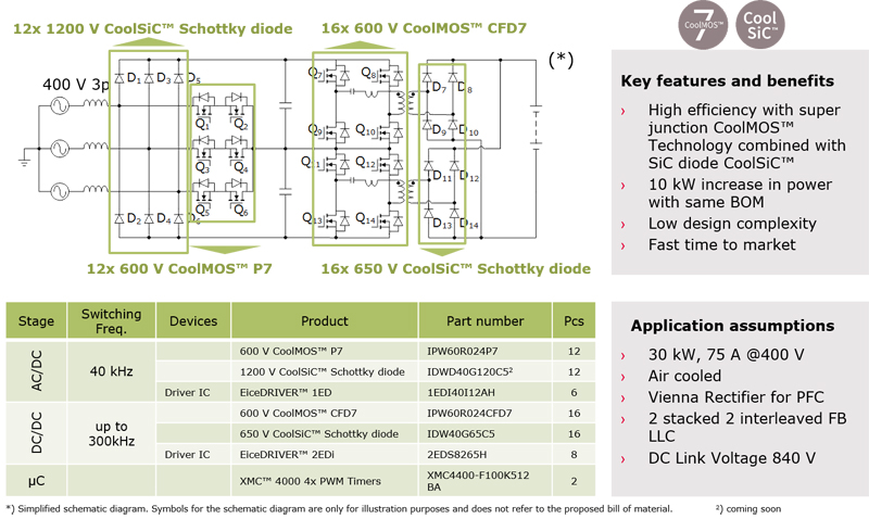
Click image to enlarge
Figure 2: Proposed design for a 30 kW charging sub-unit
As long as DC chargers are not required to feed energy back into the grid, the Vienna Rectifier makes an excellent choice for the PFC stage. This 3-phase, three level PWM rectifier requires only three active switches. Its output voltage can be controlled and it remains operational even in the event of unbalanced mains or the loss of one phase. It is also robust since, in the event of a malfunction of the control circuit, there is no short circuit of the output or the front end. The input current is sinusoidal, with various implementations being shown to achieve a Power Factor of up to 0.997, THDs of below 5 percent, and efficiencies of 97 percent or better.
Such a topology is efficiently implemented with a combination of silicon and silicon carbide (SiC) technologies. Devices such as the CoolSiC 1200V 5th generation Schottky diodes deliver temperature independent switching behaviour, high dv/dt ruggedness and a low forward voltage of just 1.25 V. This reduces overall system cooling requirements and increases system reliability while offering extremely fast switching. For efficient and cost optimised solutions, the 650 V TRENCHSTOP 5 IGBTs, with their low VCEsat and switching losses, can be paired with these diodes. Alternatively, to achieve further efficiency improvements, they can be matched with the CoolMOS P7 series in the back-to-back switching stage. These provide a significant reduction in switching losses due to their low Eoss, improved gate charge (Qg), and low RDS(on) that can be as low as 24 mΩ.

Click image to enlarge
Figure 3: Making the resonant full bridge LLC stage entirely from SiC components delivers further gains in system efficiency
The two stacked resonant full bridge LLC converters make use of CoolMOS CFD7 devices featuring a fast body diode. This provides protection during the critical operating phases of a BEV charger, specifically during start-up, in the event of a short circuit at the output, or burst mode. This ruggedness is not provided at the expense of other characteristics, with the devices delivering low Eoss, Qg, and reverse recovery charge (Qrr). The granular RDS(on) provided across the family enables selection of a “best-fit” device for each power class. The secondary rectification stage is completed with 650 V CoolSiC™ Schottky diodes.
Attaining more efficiency for 30 kW sub-units
By moving to an implementation with a higher share of SiC devices, the same topology can be made more efficient. In addition, due to the lower number of components, reliability is increased while heat generation is reduced. The high-voltage DC/DC stacked approach is replaced with parallel full-bridge LLC converters. To accommodate the higher DC-link voltages on the primary side, the switches are replaced with 1200 V CoolSiC MOSFETs. The higher secondary-side voltages are handled by upgrading the diodes to 1200 V CoolSiC devices. The combination of fewer components, together with the lower RDS(on) provided by each device, delivers lower conduction losses. Overall, sub-units taking this approach deliver a longer lifetime with higher reliability, increased power density, and enable operation at higher switching frequencies.
Selection of the optimal gate driver
The control signals from a microcontroller (MCU), such as an XMC4000, or digital signal processor (DSP) need to be linked to the power devices via a suitable gate driver. Solutions based upon silicon-on-insulator (SOI) technology with monolithic level-shift robustness and galvanically isolated coreless transformer (CT) technology provide the required performance for driving both half and full-bride stages. Critical performance measurements include the propagation delay, drive current, VS immunity, level-shift losses, and switching frequency, to name but a few.
![]()
Click image to enlarge
Figure 4: Block diagrams for the single and dual-channel coreless transformer EiceDRIVER gate drivers
The designs discussed utilise two families of the EiceDRIVER range; the 1ED and 2EDi. Solutions such as the 1EDCx0I12AH are single channel isolated CT gate drivers offered in a wide body package and are certified to UL-1577. The input side supports a wide range of voltages, simplifying connection to an MCU or DSP, as does the output side with support for both unipolar and bipolar operation. The rail-to-rail output driver simplifies gate resistor selection, saves on an external high-current bypass diode, and enhances dv/dt control in both high and low-side configurations.
The 2EDS8265H is a fast dual-channel gate driver, with isolation between both the input and output sides, as well as channel-to-channel isolation on the output side. The excellent common-mode rejection, fast signal propagation, and high drive current is well suited to the CoolMOS CFD7 and CoolSiC devices used in the primary side of the stacked LLC.
In the context of a BEV fast charger features such as active shutdown, in situations where the output device is not connected to the power supply, and under voltage lockout (UVLO) contribute to the robustness of the overall solution. In conjunction with an optimal layout, such as locating decoupling capacitors close to the input and output supply pins and reducing the parasitic inductance with ground planes, ensures good thermal and electrical (noise immunity) performance can be attained.
Summary
For BEVs to become a mode of transport that are equally at home on long-distance journeys as they are for short, inner-city use, the charging infrastructure needs to move closer to today’s experience refuelling a petrol or diesel vehicle. For this, fast DC chargers delivering up to 150 kW are part of the solution. Chargers of this dimension are taking a modular approach, combining several lower power units to achieve the desired output power.
With efficiency, reliability, thermal considerations, size and cost all under close scrutiny, it is clear that SiC devices will play an important role in developing the required solutions. These may be combined with existing silicon MOSFET switches or, where highest efficiencies need to be achieved along with a lower part count, in combination with SiC switches. Together with the appropriate gate drivers and control electronics, air-cooled 30 kW or greater modules can be realised to meet current worldwide charging standards.
Infineon technologies