Tapped Buck AC-DC Power Topology Optimises Cost in ErP-Restricted Appliance PSU Designs
When designing a medium power (10 W – 20 W), non-isolated, AC-DC power supply the choice is typically between a conventional buck topology and a more complex, flyback transformer based circuit.
The buck converter design, although simple and easy to design with, has some drawbacks. Buck converters use a simple low cost inductor for the energy storage element but require a large expensive power MOSFET, especially if the output current is in excess of 400 – 500 mA, and a high voltage (600 V) high current, fast freewheeling diode. The flyback design uses a more complex transformer in place of the inductor and requires a smaller power MOSFET and lower voltage (and therefore lower cost) free-wheeling diode. Flybacks can also provide output isolation if required.
In terms of which is most efficient – buck or flyback - that mostly depends on the input vs output voltage and current requirements. If there is a large difference between the input and the output voltage, then the flyback topology is likely to be more efficient because the turns-ratio naturally steps the voltage down, whereas the buck needs a reduced duty cycle which increases the peak currents and I2R losses. If the ratio is small, then the buck topology is likely to be better because flybacks need a primary clamp in the flyback circuit and also there are magnetization and leakage inductance losses in the flyback’s transformer core.
There is a third AC-DC converter architecture which offers reduced cost compared to the conventional buck converter design and reduced complexity compared to the flyback design, the tapped buck. Tapped buck PSUs have the benefit of a turns ratio to assist with large voltage conversion ratios and are generally more efficient than non-isolated flyback designs; up to 2% in some cases.
The tapped buck topology uses a simplified transformer which operates as an auto-transformer, where the primary and secondary are directly connected. The transformer reduces the output voltage but maintains the same current flowing through both windings. This reduces complexity, weight and cost of the transformer but does not provide the output isolation that is typically provided in a conventional flyback design. An additional feedback winding is added which ‘taps-off’ a proportion of the input voltage (similar to the secondary tap) to feed back a control voltage to the switcher. The tapped buck architecture utilizes the smaller, lower cost MOSFET and lower voltage freewheeling diode seen in flybacks. The tapped buck architecture also has the advantage of producing less stress on the switching MOSFET during commutation improving long term reliability.
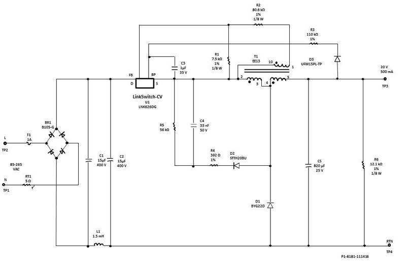
Figure 1 illustrates the schematic for an 85 VAC – 240 VAC input, 20 V 500 mA (10 W) output AC-DC converter using a tapped buck topology. This design uses Power Integations’ LinkSwitch-CV IC (LNK626DG), U1, configured as a high side driver. The schematic looks very similar to a conventional inductor-based design except that the inductor is split into primary and secondary windings, linked at a common point which is then connected to the free-wheeling diode D1. When the power MOSFET in LNK626DG switches on, the current ramps up through the transformer T1, storing energy, which flows out through the load - as is the case with a conventional buck converter. When the power MOSFET switches off, the magnetic field starts to collapse causing a reversal of the voltage across the inductor, and the stored energy is converted into a current which flows out via the load, returning via the free-wheeling diode. The peak current is stepped-up by the turns ratio between the primary and secondary windings. The feedback winding provides a control voltage which is connected to the feedback (FB) pin via a potential divider formed by R2 and R1. The feedback voltage is set by the feedback winding turns ratio and the potential divider ratio to provide the required 20 V output voltage.
The LinkSwitch-CV family integrates a wide range of protection features which make the LNK626OG ideal for energy efficient EcoSmart off-line switching power supplies. LNK626DGcan operate in continuous or discontinuous mode and compensates for external component temperature variations. ON/OFF control provides constant efficiency over a wide range of loads and retains this high efficiency at light loads, making LinkSwitch-CV perfect for applications that need to meet ErP regulations.
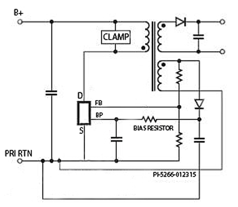
No-load power dissipation can be reduced to less than 70 mW by switching to a conventional flyback design with the addition of an external bias circuit as depicted in Figure 2.
Click image to enlarge
Figure 2. External bias for reduced quiescent power consumption
Advanced protection features include auto-restart in the event of output short circuit or control loop faults. During auto-restart, the power MOSFET is disabled for 2.5 seconds then switched on for 200 mS (8 % duty cycle). If the fault is no longer present, the part completes a normal start-up sequence. Hysteretic thermal shutdown includes automatic recovery that allows the controller to restart once the IC temperature has reduced to below 85 deg C.
During normal operation, the bypass (BP) pin is powered from the main output of the circuit through D3 and R3. Quiescent (no load) power consumption can be optimised by careful selection of R3 and C3. The leakage energy in T1 causes drain voltage spikes which are typically limited to below 90 % of the breakdown voltage rating of the internal power MOSFET. To minimise the leading-edge spikes, a snubber circuit consisting of an RCD network comprising made D2, C4, R4 and R5 is used to limit the voltage excursions and reduce stress switching element. Output ripple is controlled by the output smoothing capacitor C5. To keep the ripple below 200 mV the output capacitor needs to have low ESR.
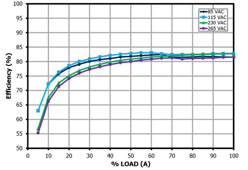
The tapped buck design illustrated in Figure 1 is based upon the Power Integrations Design Example Report DER-572 for a 10 W (12 V – 20 V, 500 mA output) AC-DC power supply. Designers using the methodology described in the report can expect to see efficiency greater than 82% from half-load to full-load, and 72 % at 10 % load for a 115 V AC supply (which drops to 67 % for a 240 V AC supply). This performance is described in Figure 3.
Click image to enlarge
Figure 3. Efficiency vs Load at room temperature measured at the Output Terminal.
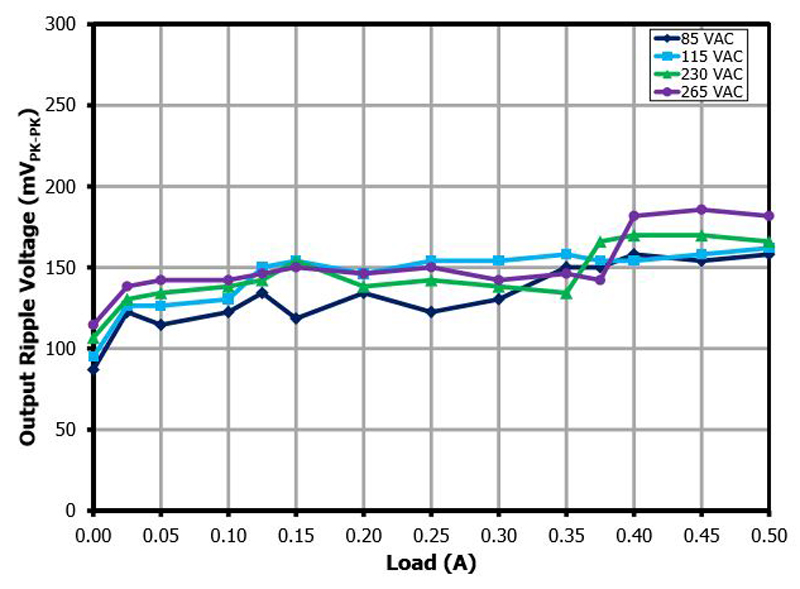
Output ripple is maintained at less than 182 mV across the load range and across the line input voltage range (85 – 265 V AC). Voltage ripple is shown in Figure 4.
Click image to enlarge
Figure 4. Output voltage ripple vs output load
DER-572, is freely available to download from the Power Integrations web site and contains all design and layout information as well as detailed instructions on how to wind the Tapped Buck transformer. Details of the full LinkSwitch family can be found on Power Integrations website.