Improving System-Level Performance and Robustness in Power Line Monitoring
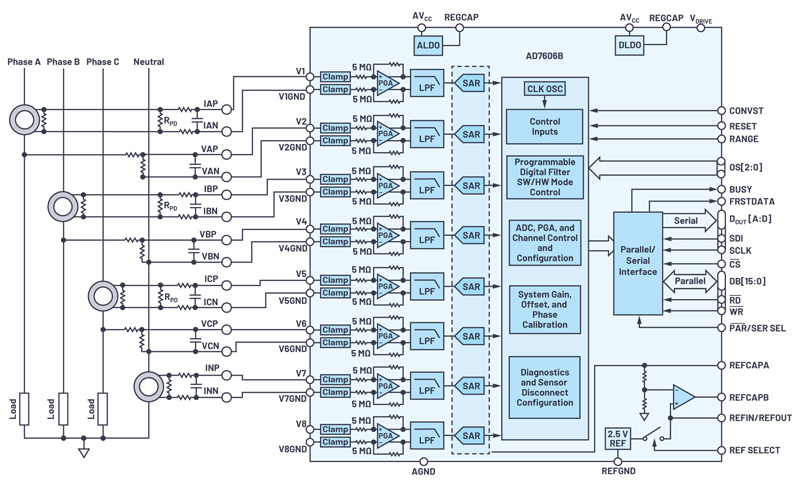
Figure 1. AD7606B in a typical power line monitoring application
For many applications, monitoring powerlines implies the use of current transformers and resistor divider networks in order to sense the three phases and neutral voltages and currents, as shown in Figure 1. The AD7606B, due to its high input impedance, can directly interface with a sensor, easing the data acquisition system design as AD7606B provides all the required building blocks.
The AD7606B integrates on-chip, eight individual signal chains that accept either ±10V or ±5V true bipolar analog input signals despite working from a single 5V supply. These features eliminate the need for driver op amps and external bipolar supplies.
Each of these channels is comprised of 21V analog input clamp protection, a resistive programmable gain amplifier with 5MΩ input impedance, a first-order anti-aliasing filter, and a 16-bit SAR ADC. Also, an optional digital averaging filter with over sampling ratios of up to 256 and a low drift 2.5V reference are included to help build a complete powerline data acquisition system.
In addition to the complete analog signal chain provided, the AD7606B has plenty of calibration and diagnostic features to improve system-level performance and robustness.
Direct Sensor Interface
Unlike AD7606, AD7606B input impedance has been increased to 5MΩ, which allows for it to directly interface with a wide variety of sensors while granting two straightforward benefits:
- The gain error introduced by external series resistors (for example, the filtering or the resistor divider network) is reduced.
- The offset seen when the sensor is disconnected decreases, allowing for easy sensor disconnect detection features.
Gain Error Due to External Resistors
In factory trimming, there is tight control over RFB and RIN (5MΩ typical) on a PGA, such that the AD7606B gain is accurately set. However, if an external resistor is placed in the front end, as shown in Figure 1, the actual gain then differs from the ideal trimmed RFB/RIN.
The higher the RFILTER, the greater the gain error becomes, which will require compensation on the controller side. But the higher the RIN, the less effect the same RFILTER will have. Unlike the AD7606’s 1MΩ input impedance, the AD7606B has 5MΩ input, meaning that the gain error will reduce about 1 over 5 for the same series resistor (RFILTER) without any calibration, as shown Figure 2.
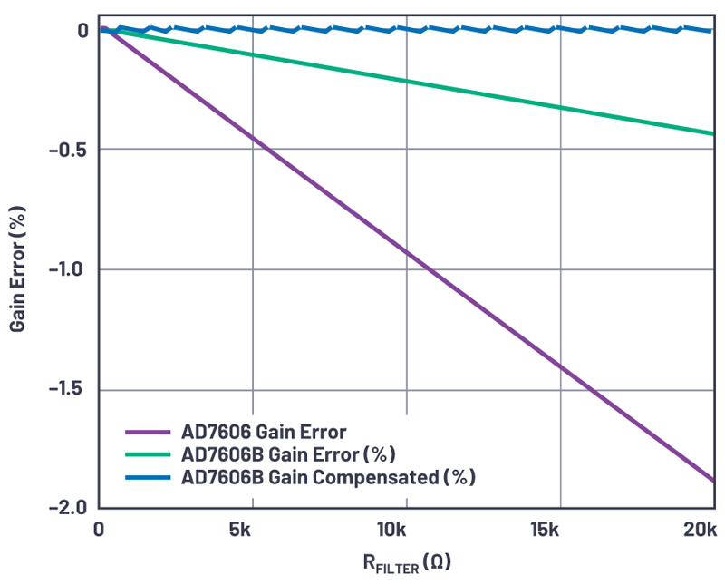
Click image to enlarge
Figure 2. Gain error introduced by a series resistor
However, by using the AD7606B in software mode, this system gain error can be automatically compensated on-chip, on a per-channel basis, and completely eliminate the need for doing any gain calibration computation on the controller side.
Sensor Disconnect Detection
Traditionally, having a pull-down resistor (RPD) in parallel with the sensor (current transformer shown in Figure 1) allows users to detect when the sensor disconnects by monitoring if an ADC output code lower than 20LSBs repeats for a number of samples (N).
It is recommended to have an RPD much larger than the source impedance of the sensor in order to minimize the error that this parallel resistor may introduce. However, the larger the RPD, the larger the ADC output code generated when the sensor disconnects, which is not desired. A large ADC output code may lead to unnoticed sensor disconnection. Because the AD7606B has larger RIN than the AD7606, for a given RPD, the ADC output code is lower if the sensor disconnects, as shown in Figure 3, reducing the risk of false alarms.
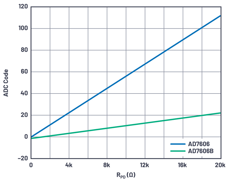
Click image to enlarge
Figure 3. Offset error when the sensor gets disconnected from the ADC’s analog inputs
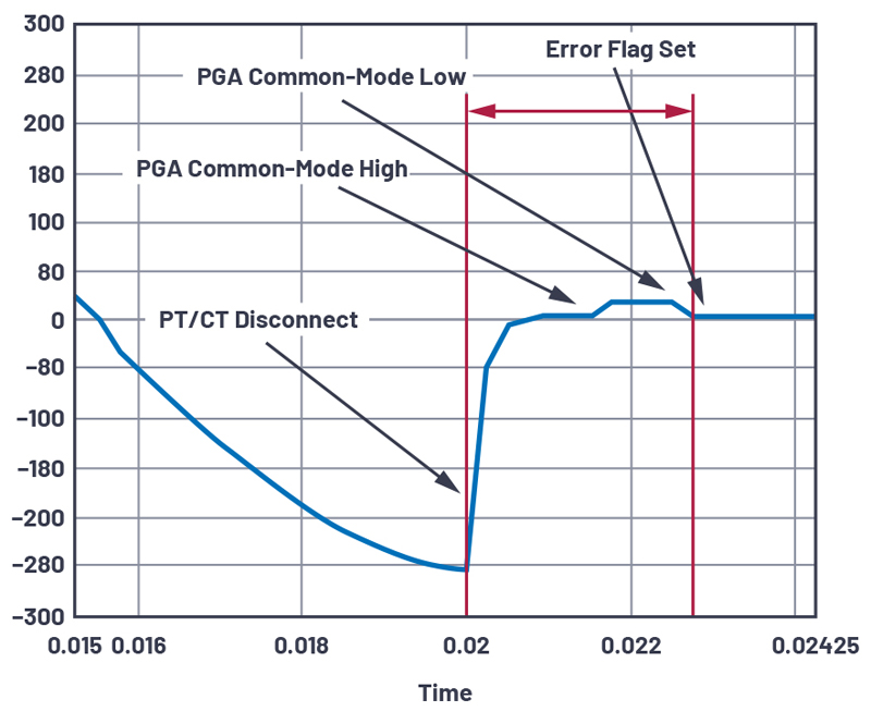
When entering software mode for the AD7606B, there is an open-circuit detection feature, eliminating the burden on the back-end software that detects the sensor disconnection. After programming the number of samples N (N=3 on the example of Figure 4), if the analog input remains for several samples reporting a small dc value, the algorithm will automatically run and assert a flag if the analog input signal has been disconnected.
Click image to enlarge
Figure 4. Sensor disconnect detection
System-Level Performance
System Offset Calibration
When using a pair of external resistors, as seen in Figure 1, any mismatch between them will cause an offset. This offset can be measured as the ADC output code when the sensor is shortcut to ground. An offset from –128LSBs to +127LSBs can be then added to or subtracted from the conversion result by programming the corresponding channel offset register in order to compensate for that system offset.
System Phase Calibration
The CONVST pin manages the start of a conversion such that it triggers the process simultaneously on all channels. However, on applications where currents are measured through current transformers (CTs) while voltages are scaled down through a voltage divider, there will be a phase mismatch between current and voltage channels. To compensate for that, AD7606B can delay the sampling instant on any channels, such that the output signals can be realigned in phase, as shown in Figure 5.

Click image to enlarge
Figure 5. Phase realignment.
System Robustness
In order to increase system reliability, several diagnostic features have been included on-chip, namely:
- Overvoltage/undervoltage comparators on every channel.
- An interface check that clocks out fixed data on each channel in order to verify the communication.
- SPI invalid read/write alerts if there is an attempt to write to or read from an invalid register.
- BUSY STUCK HIGH alerts if the BUSY line continues longer than the normal time after a conversion has been initiated.
- Reset detection alerts if a reset has been detected for either a full, partial, or power-on reset on the internal LDO regulator.
- CRC can be performed in the memory map, ROM, and every interface communication in order to guarantee correct initialization and/or operation.
Conclusions
The AD7606B brings a complete data acquisition system on a chip to the market. All the analog front-end building blocks are implemented. It provides a complete set of advanced diagnostic features, as well as gain, offset, and phase-calibration. With this, the AD7606B reduces component cost and system design complexity, easing the journey to designing powerline monitoring applications.