Increasing Multi-Output Flyback Transformer Efficiencies in Power Supply Applications
The world is moving to smaller, lighter, faster and greener energy sources. Likewise, power supplies demand a similar evolution.
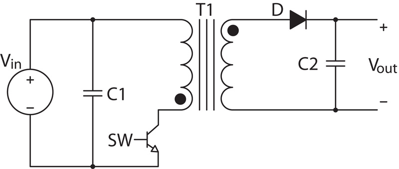
Figure 1: The flyback transformer circuit schematic
Integrated circuits and transistor components of the switch mode power supply (SMPS) already operate at faster switching speeds and higher efficiency than in previous years. Likewise, magnetic components used in SMPS circuit topologies require advanced design and analysis to keep up.
A flyback topology with low circuit component count relies on critical design and analysis of the coupled inductor or “flyback transformer” to meet new and updated requirements. Since the magnetics are typically the largest component of the circuit, the goal is reduced size at higher operating frequency and efficiency.
This article evaluates several flyback transformer designs. Analysis and measurements will be given emphasizing Litz wire to reduce AC power loss in the total coil design. Overall efficiency increases will be compiled in terms of total loss (core + coil) of the finished component.
Flyback Transformer Basics
Flyback topology in terms of the magnetics is an energy storage medium versus traditional energy transfer defies the classic definition of the word “transformer” not being one at all. In operation, it is a highly coupled inductor. The unique operation in theory then is a means to “store” energy. In magnetics design practice, it is accomplished by introducing a small air gap somewhere in the core magnetic flux path.
When the primary switch (transistor) turns on, current energy in the primary winding is stored in the core and gap via E∝LI2. E is energy, L is primary inductance and I is primary current. When the switch opens, primary winding polarity changes and the reverse-biased diode on the secondary side allows current to flow through the secondary winding. Stored primary energy moves to the secondary winding and ramps down.
To translate circuit operation to actual design, mix of hand calculations, circuit simulators, analytical tools and FEA (Finite Element Analysis) software are used. Optimization for finished products is accomplished through various iterations of core and coil design plus building and measurement of samples to verify the calculation/simulation process. Actual sample testing and measurement being most evident in this article’s focus. AC coil loss quickly moves from simple equation to matrix and series analysis to solve. Thus, the use of advanced computer tools like Ansys PEXPRT and Ansys PEMAG can provides good representation of AC losses that include eddy current skin, fringing, and proximity effects.
The initial coupled inductor design takes no high-frequency AC coil effects into consideration with subsequent designs using various winding and layering techniques that reduce AC coil resistance for reduced power loss.
Design 1: 60 W Flyback Transformer
Design specifications for a 60W flyback (Table 1) have five windings in total: one primary, three secondary and one auxiliary. To meet typical safety standards, secondary windings used reinforced insulated wire. Note: insulated wires can increase the size of the wire by up to 30 percent due to wire coating thickness. A Ferroxcube EE30 3C94 Mn-Zn ferrite core will be used.
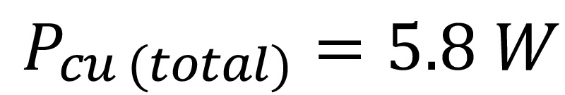
AC and DC resistance were obtained from FEA simulation. AC resistance was multiplied by RMS current squared (Table 2) with DC loss found using DC current.
Total DC plus AC copper loss, denoted Pcu was:
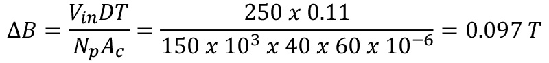
Core loss is found using flux density ripple ΔB from Faraday’s law (Equation 1.1), where Vin is the input voltage, Ac is the core area, D is the duty cycle, T the switching period and Np is the number of primary turns:

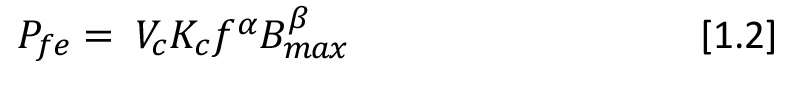
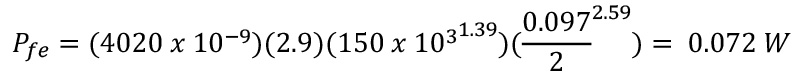
Using the General Steinmetz Equation, the core loss Pfe is calculated where Vc is the core’s volume, f is the switching frequency, Bmax is the peak flux density and Kc, αand βare Steinmetz parameters derived from core material properties:
For Design 1, the total loss Ptotal equals copper loss and core loss combined:

Core and coil loss generate heat, and heat effects through core and coil are highest at the center of the component and radiate out to the surface where convection cooling occurs.
ANSYS thermal simulation was used to estimate a target total temperature rise of 40°C for both core and coil. Ambient temperature used was 22°C. Design 1 shows a total temperature (core + coil) of 98°C and temperature rise of 76 °C. far exceeding target temperature rise. Note that coil AC resistance contributes most to copper losses. Core losses are negligible compared to the winding losses.
Design 2 and 3: The Fringing and Proximity Effects
Design 2 accounts for fringing effects by changing distance between core gap and the start of the first winding. Fringing effects cause increases in AC resistance due to the bulging of magnetic flux around the core gap versus travelling straight across it.
Distance is increased between core (gap) and coil using thicker bobbin material or using spacer tape before coil winding begins. This increases the Mean Length Turn (MLT) and thus DC resistance too. However greater reduction of AC resistance outweighs it. This technique results in an overall power loss of 4.15 W; a 30 percent reduction in copper loss. Core loss is unchanged. Thermal simulation shows total temperature 78 °C; a reduction of 20 °C but still high compared to target.
Design 3 accounts for proximity effects by reducing the number of wire layers in total coil construction. Proximity effect has a direct relation to AC resistance and occurs where current distribution in one winding layer influences distribution in another. For example, a winding has current flowing in one direction (positive) where current flowing in the next layer would be negative. The attraction of positive and negative charges alters the distribution of current so that it doesn’t travel uniformly through the conductor and bunches to one side. This affects even AC current and thus increases AC resistance.
Reducing layers reduces AC resistance of the primary winding and secondary winding 1. However, AC resistance increases for secondary windings 2 and 3 due to unavoidable bunching and uneven layering of primary and secondary 1 before the last two winds. These trade-offs show overall loss marginally better for Design 3 but still too high. Thermal simulation was not completed as total losses were only marginally improved.
Litz Wire: Accounting for the Skin Effect
While proximity and fringing effects were reduced in the above design trials, the resulting power loss reduction was not enough. AC resistance remains large. Focus is now given to wire skin effects.
A wire carrying an AC current will generates an AC field, which produces a cavitating effect called eddy currents in the wire. The effect of eddy currents impede even distribution of electron current flow in the entire cross section of a piece of wire. The cavitation effect of eddy currents pushes current (density) to the outside of the wire. As skin effects are frequency dependent, higher frequency AC current (density) won’t protrude as deep into the middle of the conductor. This is known as skin depth.
To combat this, several to hundreds of strands of smaller wire are twisted together to create a larger diameter, or gauge, single wire. Multiple wire strands reduce AC resistance loss due to skin effect. Higher frequency AC currents require more strands of wire to be used. To reduce the AC resistance, Litz wire was used on all the secondaries. Thicker wire on the windings helped reduce the copper losses. Note the design uses a standard bobbin with thinner barrel wall as fringing effect has a greatly reduced using Litz wire.
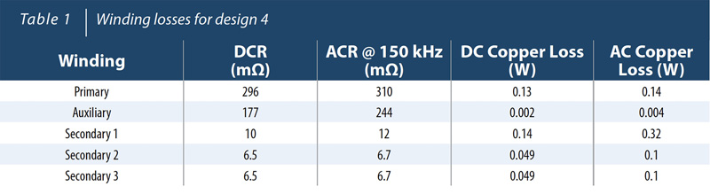
Table 1: Design 4 winding loss
Core loss remains unchanged, and total loss is less than the maximum power dissipation. Total temperature rise is now an acceptable level in a greatly improved design. The Litz wire flyback transformer design was tested in an energy storage battery charger application development board. Results are recorded in Table 2.
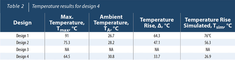
Table 2: The recorded results for Design 1 – 4.
The tests performed on the various flyback transformer designs presented in the article showed that incorporating Litz wire produced the greatest reduction in copper loss and reduced the overall temperature and temperature rise of the finished good to near target levels. Bourns tests and measurements also demonstrated that the use of Litz wire produced lower AC resistance than conventional wire and was superior to any other method applied to reduce AC resistance. This resulted in reduction of power loss for the magnetic design iterations and directly related to increased efficiency of the total power supply circuit.