Infineon Breaking Boundaries with Infineon’s New GaN Solution
Introducing the 600 V CoolGaN™ with matching EiceDRIVER™
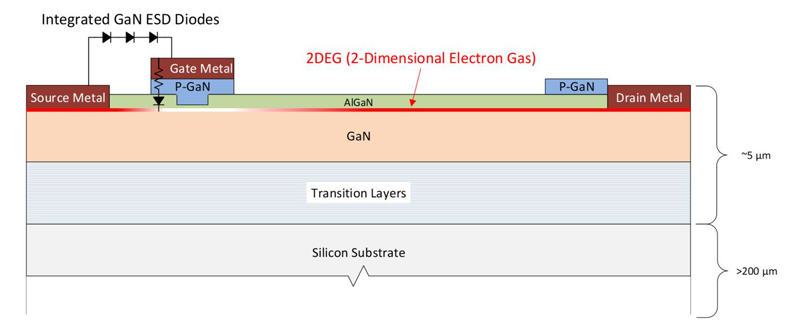
Figure 1 Cross section of a 600 V CoolGaN™ ™ power transistor [1]
Today’s demand for high-performance, low-cost power conversion products is driven by consumer expectation for longer battery life, faster charging for their phones, electric vehicles (EVs) or power tools. And consumers want faster data communication along with powerful artificial intelligence (AI) capabilities, delivered at lower cost from the vast network of hyperscale datacenters, telecom server farms, and upcoming 5G communication towers integrated into our everyday living environment. At the heart of achieving high performance as well as lowering the up-front and operating costs for these applications, is advanced power electronics that process electric utility voltage through multiple stages to ultimately power our devices efficiently and cost-effectively.
For many years this progression has been enabled by continuous innovation resulting in families of high and low-voltage silicon power transistors that never fail to surprise us with further improvements generation after generation. Now Infineon continues this innovation by introducing a family of 600 V GaN power transistors and related driver ICs at electronica 2018, the world’s leading trade fair for electronic components, in Munich. This article addresses what GaN is, what it can do for us, and provides application examples of where it is used to reliably provide ultra-high efficiency at the lowest system cost.
What is GaN and how does it work?
Gallium nitride (GaN) is a wide bandgap semiconductor material in the same category as silicon carbide (SiC). If it were possible to grow large-diameter single-crystal GaN to make wafers for processing, vertical transistors could be fabricated in a similar way as SiC MOSFETs are made today. But growing GaN substrates has proven to be prohibitively difficult. Instead it is far more effective to use readily-available, low-cost silicon wafers as a substrate, and grow GaN epitaxially so it can be fabricated into lateral transistors known as high electron mobility transistors (HEMTs).
Figure 1 shows the cross section of a CoolGaN™ ™ transistor based on this structure. Since GaN and Si have different crystal lattice constants and coefficient of thermal expansion, proprietary transition-layers are first grown to provide a suitable base on which to grow the GaN layers. At the interface between the GaN and AlGaN layers, a sheet of free electrons, known as a 2-dimensional electron gas (2DEG) is formed. The 2DEG is highly conductive due to the exceptional electron mobility of this layer. Drain and source contacts can be added, and a gate structure that provides a local electric field is used to deplete or enhance the 2DEG, enabling the 2DEG to essentially be turned on and off. Using p-doped GaN for the gate makes this an enhancement, rather than depletion-mode device – in other words, it is normally off, with a gate threshold of about +1.4 V.
Note the diodes shown on the gate structure. This combination of Titanium gate metal and p-GaN forms an ohmic contact in series with a GaN diode between the gate and source. The diode has a knee voltage of about 3.5 V in the forward direction. In addition, 3 series GaN protection diodes are monolithically integrated onto the GaN transistor to protect the gate from electro static discharge (ESD). These ESD diodes begin clamping when VGS goes more negative than about -10 V. In this way, the gate voltage of CoolGaN™ is self-clamping by integrated diodes in both the forward and reverse direction, making it extremely rugged and immune to overvoltage spikes. Competitor’s enhancement-mode GaN structures use a Schottky gate contact, which blocks the GaN diode clamping function. As a result, the competitive devices require external circuits to manage and limit gate voltage transients which would otherwise damage the Schottky gate and lead to failures. Figure 1 also shows the p-GaN “hybrid drain” structure that effectively manages trapped charge, thus mitigating dynamic RDS(on) variations that can plague competing GaN transistor design approaches (refer to ref. [1] for further details).
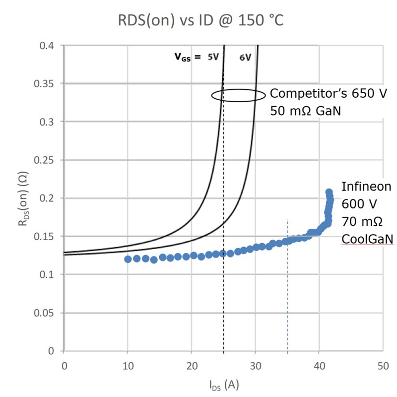
Another key competitive advantage of CoolGaN™ is its higher saturation current capability, especially at maximum temperature (150°C) where it matters most. Figure 2 compares a 70 mΩ-rated CoolGaN™ transistor versus a competitor 650 V, 50 mΩ-rated transistor [2]. Even when driven to the maximum recommended gate voltage of 6 V, the competitor’s GaN is rated to only 25 A maximum. In contrast, the CoolGaN™ device is not only lower RDS(on) over the entire current range, but it is rated at 35 A maximum drain current, 40% greater than other devices in the market. This peak current handling capability is critical because many applications require the device to operate/survive in transient high-current conditions (startup, line-cycle dropout, lightning-strike transient, short-circuit faults, etc.). This combination of a rugged gate structure and higher peak current handling capability helps make Infineon’s CoolGaN™ the most rugged and reliable GaN power transistor on the market today.
Click image to enlarge
Figure 2 Comparing saturation current of CoolGaN™ ™ versus competitor
Driving GaN – what is different about driving the gate?
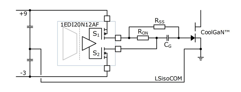
As described in the previous section, the CoolGaN™ ™ gate is self-clamping with a forward voltage of approximately 3.5 V. So instead of driving the gate-source with a fixed voltage, the gate is ideally driven with a current source, and the resulting voltage on the gate simply follows the diode characteristic. For the 70 mΩ device described above, the typical steady-state gate current to fully enhance the gate is about 10 mA. But in order to quickly charge the gate capacitance, a much higher pulse current is necessary for about 20 ns. A 2-stage current-source driver could accomplish this, but a much simpler solution is to use a conventional gate driver with an R-C network to the gate (instead of the conventional R), as shown in figure 3. With this simple circuit, a conventional 12 V gate driver can be used to effectively drive the GaN gate. Not only does the RC network provide the pulse of peak current necessary to achieve fast turn-on, but it also then charges-up to VCC – VGS, and that charge results in a negative gate bias at turnoff.
The negative bias is actually beneficial as it provides additional margin to prevent spurious gate turn-on due to fast positive dv/dt on the drain (a C dv/dt induced turn-on due to the current injected by the gate-drain capacitance). The negative bias can be supplied by a fixed negative supply to the gate driver, and/or negative bias supplied by the capacitor in the RC network.
Click image to enlarge
Figure 3 Simple gate drive method using IGBT gate driver
But constant negative gate bias voltage has a disadvantage: when the GaN transistor conducts in the reverse direction during dead time between high and low-side conduction, the effective voltage drop is approximately 2 V plus the negative gate bias. Therefore it is desirable to use only the smallest negative bias necessary to keep the gate fully turned-off, in order to minimize power dissipation when in third-quadrant conduction (diode mode) during dead time. Ideally, VGS would return to zero after the dead time.
Click image to enlarge
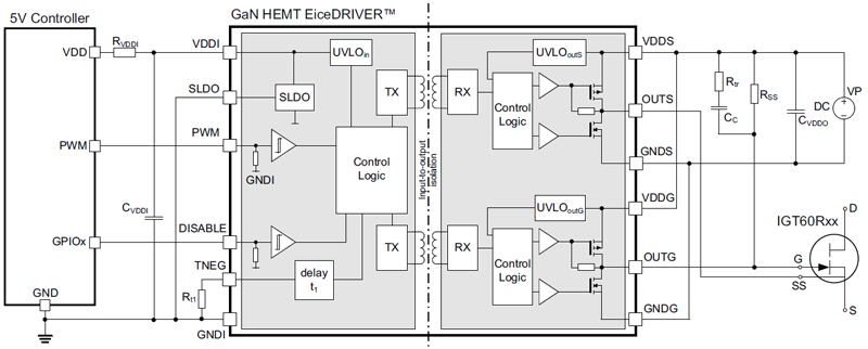
Figure 4 The new high-performance EiceDRIVER™ isolated GaN gate driver
This is where the new Infineon 1EDF5673 EiceDRIVER™ isolated gate driver comes-in. The 1EDF5673 and its 1EDS package variants all feature a unique three-level gate drive solution shown in figure 4, with the waveforms in figure 5. The new driver is among the fastest isolated drivers offered by Infineon, with a 37 ns propagation delay and a -6/+7 ns delay uncertainty for highly accurate driver timing necessary for adaptive dead time management at high frequencies. Moreover, the driver has a common mode transient immunity (CMTI) of >200 V/ns to handle the high switching speed that GaN transistors are capable of. This driver operates from a single supply voltage, but provide negative gate drive temporarily from the RC capacitor, or by inverting its output during startup or burst-mode. Otherwise the gate voltage is returned to zero to optimize the GaN third quadrant conduction at all other times. The negative drive duration is programmable with a resistor on the TNEG input pin. These operational modes provide the best combination of speed, performance, and safety from spurious turn-on in any GaN gate driver available today. To accommodate smaller PCB layouts requiring only functional isolation, the driver is offered in both a 5x5 mm LGA and a 16-pin narrow-body DSO – as well as a 16-pin wide DSO fully rated for UL/VDE safety isolation.
Click image to enlarge
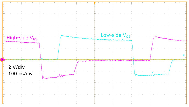
Figure 5 The three-level gate drive waveforms provided by the new GaN EiceDRIVER™
Applications – where GaN delivers highest performance:
The first instinct for any power electronics design engineer is to try substituting a new GaN device for their existing CoolMOS™ – to see how much better it performs. But they are often disappointed that GaN only provides a modest improvement in switching loss. Why is that – why doesn’t GaN necessarily provide a big improvement when dropped-into an existing circuit design? It is because these circuits where CoolMOS™ is commonly-used are often unipolar topologies like traditional boost PFC, single-ended flyback or two-transistor forward converter. In these topologies, the common-theme is that the transistor only conducts in the forward direction. Thus, the body-diode performance is irrelevant because the transistor never conducts in the third quadrant. So the only parameters that really matter besides RDS(on) are the turn-on energy loss EOSS, and the switching speed, and the small advantage of GaN here would not be worth the benefit – CoolMOS™ is already a proven technology and does a great job in these applications.
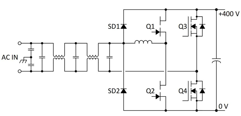
So, if not unipolar topologies, where does GaN work best and provide the most benefit? It is commonly believed that GaN is at its best at high-frequencies. Yet it can offer extraordinary efficiency in half-bridge based topologies even at modest operating frequencies like 65 kHz. Shown in figure 6 is the full-bridge totem pole PFC topology [3] used in Infineon’s 2.5 kW GaN PFC reference design.
Click image to enlarge
Figure 6 The full-bridge totem pole PFC topology
When operated in continuous conduction mode (CCM) transistors Q1 and Q2 operate alternately as boost switch and synchronous rectifier under hard-commutated turn-on conditions. If conventional silicon high voltage power transistors were used for Q1 and Q2, the reverse recovery characteristic of their parasitic body-diodes would incur huge switching losses leading to their destruction. But GaN transistors have zero reverse recovery, as there are no minority carriers involved in channel conduction. Thus the switching losses are quite low, especially since the output capacitance, and related energy is smaller than any competing transistor technology.
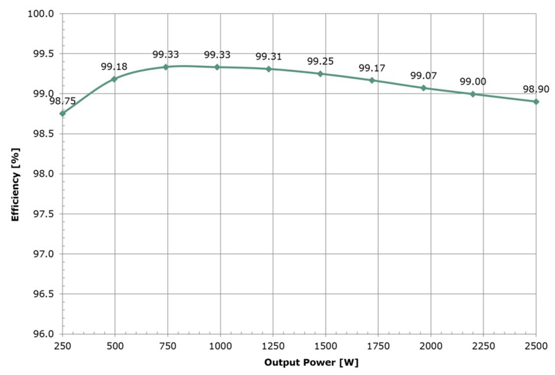
The losses are so low, that the PFC circuit shown in Figure 6 can deliver efficiencies exceeding 99% over most of their output power range, as shown in the measured efficiency plot in figure 7. The 99.3% peak efficiency is truly extraordinary, representing only 7 Watts of loss when operating at 1 kW output. This PFC circuit is a real-world reference design from Infineon that passes all of the normal PFC requirements including EN5022 conducted EMI, line-cycle dropout, and lightning-strike surge tests.
In summary, Infineon’s new CoolGaN™ offering represents the most rugged 600 V high-performance GaN transistors available today. When combined with Infineon’s coreless-transformer isolated EiceDRIVER™ gate driver family, power electronic engineers can now cost-effectively deliver higher performance power converters than ever before possible using conventional silicon transistors.
Click image to enlarge
Figure 7. Measured efficiency of Infineon 2500 W GaN totem pole PFC demonstration board
The new Infineon GaN transistors introduced today are the 600 V, 70 mΩ IGx70R060D1 available in 4 different surface-mount packages including top- or bottom-side cooled DSO, TOLL, and 8x8 DFN. In addition a 190 mΩ version in the TOLL package is offered. The product line will soon grow to cover the range of 35 mΩ, up to 340 mΩ in the same range of four packages.
References:
[1] S. Kaneko et al., "Current-collapse-free operations up to 850 V by GaN-GIT utilizing hole injection from drain," 2015 IEEE 27th International Symposium on Power Semiconductor Devices & IC's (ISPSD), Hong Kong
[2] GaN Systems GS66508B datasheet, rev. 160202
[3] J. C. Salmon, “Circuit topologies for PWM boost rectifiers operated from 1-phase and 3-phase ac supplies and using either single or split dc rail voltage outputs,” APEC, Mar. 1995, pp. 473–479