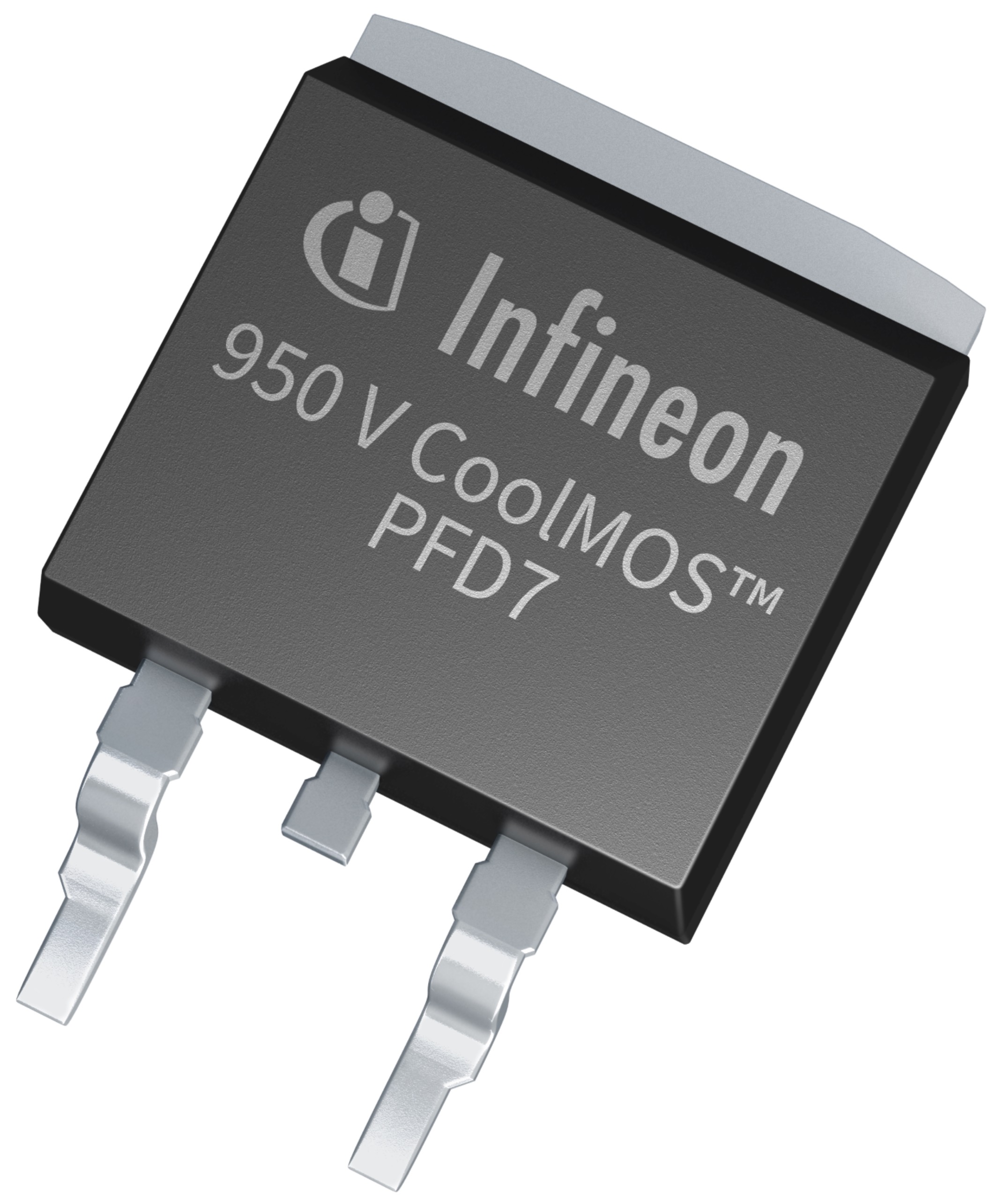
Infineon Launches New 950 V Superjunction MOSFETs
To address contemporary market needs for improved form factors and energy-efficient products, Infineon Technologies has developed a new CoolMOS PFD7 high-voltage MOSFET family, setting a new benchmark in 950 V superjunction (SJ) technology. The new 950 V series combines outstanding performance with state-of-the-art ease of use and features an integrated fast body diode ensuring a robust device and in turn reduced bill-of-material (BOM). Tailored to ultrahigh-power density as well as the highest efficiency designs, the new products are primarily addressing lighting systems, as well as consumer and industrial SMPS applications.
The new products are suitable for flyback, PFC, and LLC/LCC designs, including half- or full-bridge configurations making commutation robust and reliable. By integrating an ultra-fast body diode with ultra-low reverse recovery charge (Q rr), they offer hard commutation ruggedness and reliability. This makes it the most robust SJ MOSFET in this voltage class, enabling usage across all topologies in the targeted applications. In addition, significantly reduced switching losses (E OSS, Q OSS, and Q g) improve efficiency in hard- and soft-switching applications and result in up to 4°K lower MOSFET temperature compared to 900 V CoolMOS C3 SJ MOSFET. The new products improve light- and full-load PFC efficiency by more than 0.2 percent while matching the performance with regards to LLC efficiency, contributing to a greener world.
The new family offers up to 55 percent lower on resistance (R DS(on)) devices in various SMD and THD packages, like 450 mΩ in DPAK or 60 mΩ in TO247. This enables designers to use smaller packages and boost power density and board space savings at reduced BOM and production costs. A gate-source threshold voltage (V (GS),th) of 3 V and smallest V (GS),th variation of ±0.5 V, makes the new devices easy to design-in and drive, leading to increased design freedom. Due to the low threshold voltage and tolerance, MOSFET linear mode operation is avoided while allowing lower driving voltage and reduced idle loss. Additionally, a 60 percent improved gate charge compared to CoolMOS C3 results in significantly reduced driving losses. ESD ruggedness is ensured with a human body model (HBM) level of class 2, providing reduced ESD-related failures and improved manufacturing yield.
Availability
The new 950 V CoolMOS PFD7 family comes with exceptional portfolio granularity, with SMD and THD packages to enable smaller form factors with an increased power density and BOM savings. All product variants can be ordered now. More information is available here.
 PDF
PDF