Simple-to-use, digital-input, integrated GaN power solutions deliver higher efficiency and lead to greater power density
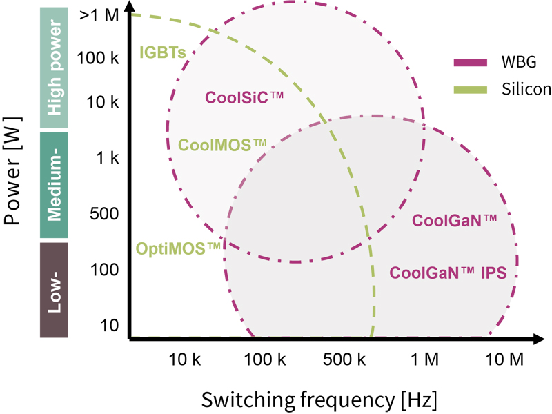
Figure 1. WBG and silicon power switch Infineon brands positioning
Introduction
Today’s switch-mode power supplies (SMPS) are smaller, more efficient, and lower-cost than ever. The key to their performance is the power switch technologies at their heart – but how should designers choose the right material for this and find the best component to meet their needs?
While silicon is the most widely-known constituent of semiconductors, a new group of wide bandgap (WBG) materials is increasingly finding its way into applications. One example is gallium nitride (GaN), which has been used for many years in high-frequency RF (radio frequency) systems and is now provided for mid- and high voltage power switches solutions since a couple of years.
More recently, GaN has become a popular choice for switching transistors in power electronics. Figure 1 shows where wide bandgap (WBG) technologies will become the component of choice. GaN transistor Figure of Merits (FoMs) enable power supplies to deliver better efficiency, with higher switching frequencies and greater power density at better robustness.
This article outlines why GaN materials are becoming more widely used in power electronics and what benefits they can bring. The most recent integrated power solutions that can provide an appealing alternative to classic discrete components are examined. Additionally, a selection guide to Infineon’s GaN discrete- and integrated system solutions is provided to help system designers make the best power switch technology choice. Depending on the application, high-, medium-, and low-power GaN product options are discussed with their different flexibilities and integration levels. Finally, to save design time, Infineon’s demo board offerings are referenced that allow an easy and quick setup and benchmark of the GaN solutions.
The benefits of GaN
The GaN High Electron Mobility Transistor (HEMT) has some key advantages over silicon for power devices. Specifically, GaN HEMT FoMs have:
-
lower and more linear behavior of output parasitics COSS,
-
10 times lower gate capacitance Cg,
-
zero reverse recovery losses due to lack of the classic MOSFET body diode, and,
-
higher mobility of the electrons (holes) in the channel that enables RON*Area [mm2] with faster switching speeds at lower switching losses combined with an excellent dynamic on-state resistance.
These make GaN HEMT an excellent choice for high-speed switching, enabling power savings and total system cost reduction due to the reduced size of external inductors or capacitors needed. It allows a higher operating frequency, which improves the power density as well as the overall system efficiency. In high-frequency operations, up to one MHz, switching speed is vital to determining how energy is transferred. The superfast switching speed of Infineon’s CoolGaN™ components, for example, enables a very short dead-time, thus improving efficiency.
Arguably, one of the most important and distinguishing features of a GaN power transistor is its ‘reverse recovery’ performance. Since Infineon’s CoolGaN™ transistors have no minority carriers and no body diode, they do not exhibit a reverse recovery. Thus, there are no resulting power losses in most of the commonly-known hard-switching totem pole (half-bridge) topologies – helping to maximize efficiency.
The second most distinct feature of the GaN wide-bandgap (WBG) material vs. MOSFETs is that the GaN does not have a hard breakdown voltage like MOSFETs. The 600 V/650 V GaN HEMT can sustain larger transient (short-term) overvoltages of above 750 V and will not have an avalanche breakthrough which could lead to an immediate electrical overstress (EOS) as in MOSFETs. This is one of the reasons that makes them more robust than their silicon counterparts. In datasheets, the tested devices have been qualified with 750 V for short transient pulses more than 10 million times.
Further, the GaN HEMT WBG reliability and qualification are done in accordance with the newly 2019 released JEDEC standards: JEP180 (Methods & Procedures), JEP173 (Dynamic On-Resistance test method for GAN), and JEP182 (Test methods for lifetime and continuous switching of GaN).
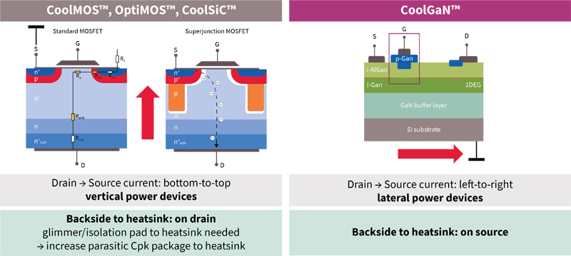
Figure 2 shows how a GaN HEMT, such as Infineon’s CoolGaN™, has a lateral conducting channel between its source and drain, as opposed to the vertical channel of conventional silicon MOSFETs. With lateral integration, future GaN HEMT Integrated Power Stages (IPS) will have higher smart functionality due to the monolithic integration capability. Further, one should keep in mind that the backside of the GaN material is on the source (ground) compared to classic MOSFETs. This has the advantage of reduced parasitic package capacitance (Cpk), simpler package integration, and in some cases, it eliminates the isolating thermal interface material to the heatsink of classic MOSFETs with drain (active high voltage (HV) side) on the backside.
Click image to enlarge
Figure 2. Lateral power switch technology
CoolGaN™ HEMT, due to the very robust ‘p-Gate’ structure, saves bill-of-material (BOM) costs via eliminating the additional two clamping z-diodes, typically seen in classic Schottky gate inputs. The input is still very simple to drive with classic gate drivers with three discretes Rg, RSS, CON (RRC, see Figure 3). The classic gate resistor Rg is for slew rate control (dV/dt), the steady-state resistor RSS is for keeping the channel open with 5 mA to 25 mA forward current, and the CON capacitance is for fast negative turn-off impulse and safe turn-off due to the low Vth GaN HEMT without any risk for re- turn-on (for dimensioning, see Infineon’s Application note “Quick-reference guide to driving 600 V CoolGaN™ HEMTs”).
For high-power SMPS (much greater than 1-2 kW) and in the case of working with the lowest RDS(ON) and the lowest Rth discrete GaN power packages, Infineon’s family of EiceDRIVER™ s gate drivers is recommended. There are dedicated functional- and reinforced- isolated GaN EiceDRIVER™ (1EDF56xx), with fast, highly accurate, stable timing and high common-mode robustness (greater than 150 V/ns).
Why further integration?
Infineon’s CoolGaN™ is already a well-established, reliable, high-performance technology for discrete products. A new, first series of single-channel and half-bridge, high-voltage, true normally-off CoolGaN™ Integrated Power Stage (IPS) products with integrated drivers was recently introduced.
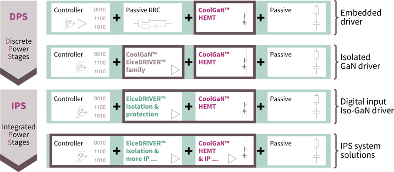
Figure 3 depicts a simple-to-use product guide of different integrated and discrete system solutions with GaN. It shows the different increasing levels of power integration and how multiple functions are available at different package integration densities. The first line shows a controller and power switch, along with suitable passives. The second and third stages show how adding a suitable isolated GaN (iso-GaN) driver increases and suits primary- and secondary- side controlled topologies, high-power system integration. The third and fourth line shows a true IPS system solution, starting with the simple-to-use IPS including the gate drive up to the application-specific integrated system solutions which will encompass the controller for specific topologies.
Click image to enlarge
Figure 3. From flexible discrete to application-specific IPS system solutions
Why is integration significant? CoolGaN™ IPS technology combines one or more CoolGaN™ normally-off GaN switches with a dedicated EiceDRIVER™ gate driver. These parts are integrated into a single QFN package, saving PCB space to help achieve small form factor designs and reduce overall costs. The integration makes it quicker and easier to design, thus reducing time-to-market.
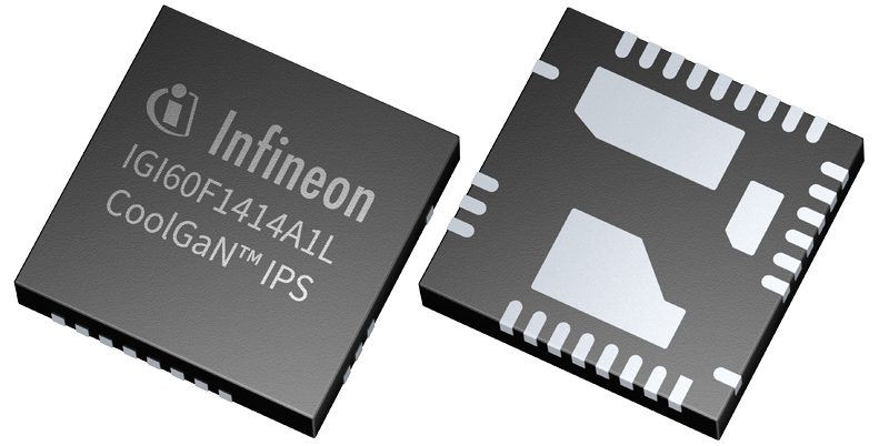
Let’s look at an example, the CoolGaN™ IPS half-bridge 600 V. This combines a half-bridge power stage, consisting of two 600 V CoolGaN™ switches, with dedicated gate drivers and suitable isolation, in a compact 8x8 mm2 QFN-28 package (see Figure 4).

Click image to enlarge
Figure 4a. Half-bridge CoolGaN™ IPS block diagram
Click image to enlarge
Figure 4b. offered in an 8x8 mm2 QFN package
The CoolGaN™ IPS family includes functional isolated PWM inputs on both the single-channel and dual-channel devices. The single-channel device is targeted at SMPS power stages from 100 W up to about 1 kW. The dual-channel half-bridge device is aimed at high-density USB charger/adapter applications.
Each product is optimized for higher power and density while remaining as simple as possible to add to a product design. For example, power-islanding PCB design techniques minimize interference to the digital power domain. Similarly, truly galvanic isolated gate drivers keep electromagnetic interference (EMI) as low as possible for robust operation.
For design engineers, the integration of CoolGaN™ IPS offers robustness, timing accuracy, simplicity and eliminates the time and effort otherwise needed to select a gate driver. Designing their system is as straightforward as possible: effectively, they just need to supply appropriate digital PWM inputs, and power is output.
The component count in the bill of materials (BOM) is reduced, as there is no need for an additional isolator IC to drive a boot-strapped high side. Additionally, the switch node parasitic inductance inside the package and on the PCB is small.
Applications for integrated GaN power devices
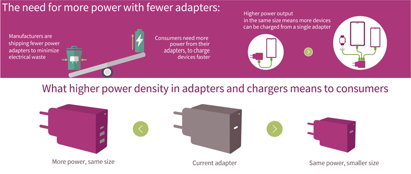
One of the most important consumer markets for power supplies is the low-power USB-PD charger and adapter segment. The chargers shipped with smartphones have been getting smaller and lighter over the years. They can provide more power from a device of the same size to charge devices faster or charge multiple devices from one adapter. Other rapidly GaN-solutions adopting markets are in power supplies for LCD TVs, motor drives, and lighting. High power density and higher power conversion efficiency prevail in these markets.
How are this improved performance and reduced size achieved? These are ideal markets for an integrated solution such as CoolGaN™ IPS. The system costs must be minimized for price-sensitive consumers, and achieving the smallest possible charger is a competitive advantage for product vendors. Moreover, there’s a requirement for surge robustness, safety isolation, and CE (EMI) and USB compliance.
For a high density, universal, USB-connected charger/adapter, the IGI60F1414A1L CoolGaN™ IPS can be used in either an active clamp flyback (AC-FB) or asymmetrical resonant half-bridge (ASHB-FB) topology. The IGI60F1414A1L is provided in a single 8x8 mm2 package, significantly reducing the PCB space required compared to discrete components.
Run in soft-switching, in both topologies, the leakage energy is recovered, which gives them a 1 percent or more efficiency gain compared to single switch topologies. 1 percent may not sound that much, but it’s a big win for this kind of application. In practice, the CoolGaN™ IPS can achieve around 95 percent efficiency for lower power outputs up to around 75 W. Above 75 W, this efficiency figure typically drops slightly to around 93 percent.
Continuing the theme of integration, Infineon is providing a complete product portfolio for a USB-PD charger system solution. This includes CoolMOS™ and CoolGaN™ power switches, as well as standalone EZ-PD™ USB protocol controllers.
Click image to enlarge
Figure 5. Trends in chsrger/adapter applications
For low- to mid-power markets, CoolGaN™ IPS really comes into its own. When higher power is required, discrete power stages (DPS) often provide the best solution, for example, for ultra-thin OLED TVs, home appliances, and high-power industrial, data center, and telecom applications.
Evaluation board saves design time
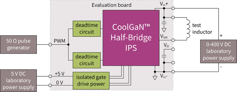
To help designers get started with CoolGaN™ IPS, Infineon offers the evaluation board, EVAL_HB_GANIPS_G1 (see Figure 6), enabling the easy and quick setup and test of a CoolGaN™ IPS half-bridge.
Using an external inductor, designers can configure the half-bridge topology of the evaluation board for boost or buck operation, pulse testing, or continuous full-power operation at power levels up to 100 W and frequencies up to the 1 MHz range. The board provides direct access to the logic inputs of the CoolGaN™ IPS chipset to drive the chipset with an external microcontroller or digital signal processor.
The evaluation board means users don’t have to design their own gate driver and power circuits to evaluate GaN transistors, thus saving valuable time.

Click image to enlarge
Figure 6. EVAL_HB_GANIPS_G1 evaluation board
Figure 7 shows a typical application example using the evaluation board for double-pulse testing. The 5 V power supply provides the circuit power, which powers the IPS logic and the isolated gate driver power supply. The DC bus voltage is provided by a 0-400 V power supply, and the input pulse width modulation (PWM) signal is provided by a lab pulse generator. A test inductor is required to connect from the DC bus to the switch-node output, and an oscilloscope can then be used to observe and measure the inductor current, switch-node voltage, or any other signal on the board.
Click image to enlarge
Figure 7. Typical application example of the evaluation board (double-pulse test)
Conclusion
Infineon is determined to provide the full range of technologies for discrete power switches: CoolGaN™, CoolSiC™, IGBT, CoolMOS™, and OptiMOS™. The technology choice of the proper component depends on many criteria.
While it is tempting to see GaN HEMTs for high-frequency designs, the overall benefits of the GaN FoMs enable and drive a replacement of past power switch technologies at existing or marginally increase switching frequencies today.
Taking integration density and lowest parasitics one step further in low- and mid-power applications, another option is to use the newly introduced, simple-to-use, integrated power components, such as Infineon’s CoolGaN™ IPS, which includes CoolGaN™ power switches and an appropriate driver offering with the lowest parasitics and best controllability of rise and fall times (dV/dt, dI/dt).
It’s always going to be down to the system design engineer to pick the best solution, but using integrated power components makes a compelling case. They can deliver excellent efficiency, robustness, high power density, and valuable PCB space savings.
Keep an eye on Infineon’s CoolGaN™ IPS webpage for the next level of higher integration innovations and feature enhancements with the upcoming product announcements or consult regional offices for more information. Alternatively click here and stay tuned – we will send latest news straight to your inbox.