As processors, such as FPGAs and MPUs, become more sophisticated, so does the need to provide multiple power rails at lower supply voltages
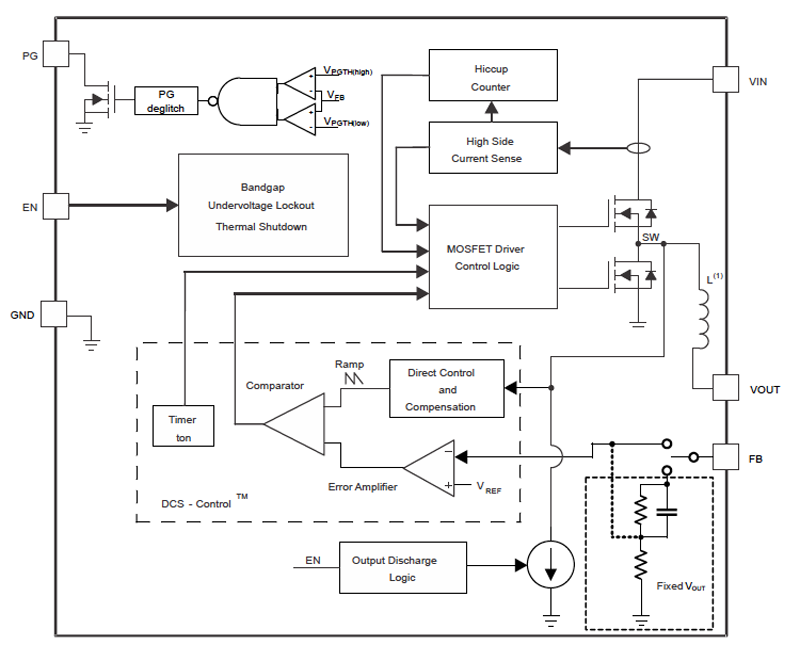
Figure 1: The functional block diagram of the TPSM8282xA buck converter range (source TI)
Processors are increasingly highly integrated devices. Squeezing more functionality into a single package offers optimal PCB space use, optimises BOM cost, and eases power management challenges. This approach is good news for many applications, from inference at the edge, compute-intensive search acceleration and industrial automation cobots. However, as the processors, such as FPGAs and powerful MPUs, become more sophisticated, so does the need to provide multiple power rails. At the same time, processor cores and peripheral functions are trending towards using lower supply voltages. High spec processors are also highly susceptible to voltage transients and ripple, requiring strict attention to the power architecture and routing power tracks around a PCB.
This article will highlight how high density, compact, low power single output DC/DC converter modules offer a viable solution.
Processor Trends
As processor geometries continue to shrink, the trend is towards increasing the functional integration within processors and programmable logic devices. System on chip (SoC) and system in package (SiP) ICs are becoming an increasingly popular method of meeting the space-constrained demands with complex and sophisticated applications.
Microcontrollers, microprocessors, field-programmable gate arrays become packaged alongside wireless LAN radios, high-speed networking transceivers, and encryption acceleration engines.
Squeezing more functionality on a single IC die has many benefits. However, the market demand for low power consumption, the ability to turn off discrete functions, and maintain application responsiveness places a significant burden on architecting the power delivery.
Power Delivery Challenges
Complex FPGAs, processors, and custom application-specific ICs require multiple power supply rails with different voltage levels, high dynamic currents, and strict adherence to regulation and transient tolerances. These highly integrated devices also require power rails to be sequenced in a pre-defined order at start-up to avoid abnormal application behaviour or internal damage.
DC/DC converters are a popular method of providing power to power-hungry devices and form part of a distributed bus or point of load architecture.
For power architects, the design constraints include board space, thermal management, sequencing power rails, and routing power.
Managing board space:Today's space-constrained applications demand optimal use of PCB space. Those with the smallest footprint are preferred when selecting a DC/DC converter. However, there are several interrelated constraints in addition to the device's dimensions, as highlighted below.
Thermal management:A converter's power density and efficiency are vital specifications to investigate on the datasheet. A conversion efficiency greater than 94% is typical, but this may still result in waste heat needing dissipation depending on the amount of output current drawn. Does the converter require special pads, mounting, or heatsinks.
Managing transients and power routing:Routing power around a PCB may expose the rails to EMI from other devices and signals. Also, long traces may result in voltage transients on large PCBs as current peaks occur. One approach to reducing the impact of transients is to place the DC/DC close to the power input pin of the device it is powering. This method is preferred subject to accommodating the converter's thermal constraints and available PCB space.
Sequencing power rails:To achieve this, a host processor requires access to a power enable pin on the selected DC/DC converter. Ideally, the converter should also feature a 'power good' output to confirm the satisfactory operation.
TI TPSM82xx DC/DC Buck Converters
Two recent additions to the TI TPSM82 series include the TPSM8282xA family and the TPSMS8286xA family.
TPSM8282xA
The TPSM82821A, 822A, and 823A are low profile, small buck converter modules with an integrated inductor and offer a single 1 A, 2 A, or 3 A output with the alternative of pin-compatible power-save mode versions TPSM82821, 822, 823. Figure 1 illustrates the functional block diagram of the TPSM8282xA range.
The converter utilises a DCS-control topology that provides an accurate output voltage with fast line and load transient response with a seamless transition between its PWM and power-saving modes. The option of a forced-PWM variant minimises output ripple by operating the converter in a continuous conduction mode across all whole load range. An enable pin, power good output, an integrated soft-start, and short circuit protection are just some of the TPSM8282xA features.
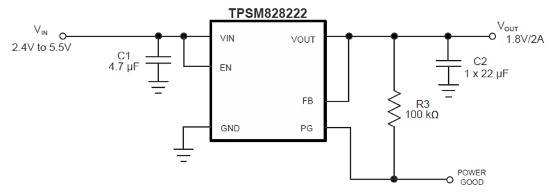
Using a potential divider, the variable output voltage range covers from 0.6 VDC to Vin, and fixed output voltage options include 1.2 VDC, 1.8 VDC, 2.5 VDC, or 3.3 VDC. Figure 2 illustrates a typical fixed 1.8 VDC 2 A converter implementation.
Click image to enlarge
Figure 2: A typical application circuit layout for the fixed 1.8 VDC output TPSM828222, 2 A DC.DC converter module (source TI)
Quiescent current falls to 4 µA. Typical conversion efficiency is up to 95%.
Supplied in a 10-pin microSiP module package, measuring 2.0 mm x 2.5 mm x 1.1 mm, the low profile, small form factor TPSM8282x family are ideal for providing power close to a processor's Vin pin.
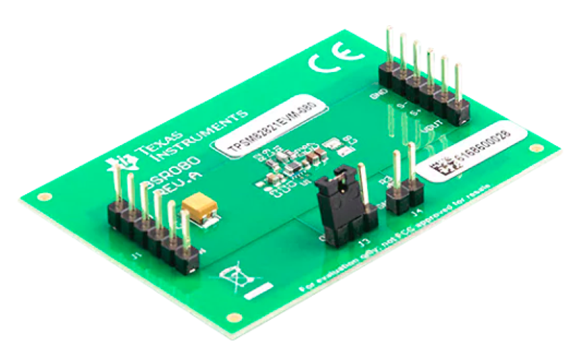
To simplify prototyping a TPSM8282x design, the TPSM8282xEVM-080- see Figure 3 - evaluation board provides a convenient platform.
Click image to enlarge
Figure 3 - The TPSM8282xEVM-80 evaluation board (source TI)
TPSM8286xA
With similar features to the TPSM8282xA family, the TPSM8286xA buck converter family consists of a 4 A module (TPSM82864A) and a 6 A module (TPSM82866A). With an energy efficiency of up to 96 %, the converters include an integrated inductor and accommodate a 2.4 VDC to 5.5 VDC input range. They are available in 13 fixed output voltage versions, covering the popular nominal voltages or a configurable output voltage from 0.6 V to Vin.
The TPSM8286x converters are packaged in an ultra-low over-moulded QFN format measuring 3.5 mm x 4.0 mm x 1.4 mm (-826xA) or 1.8 mm (-828xAH). A large thermal pad on the underside of the QFN package and its high efficiency contributes to excellent thermal management characteristics for such a compact converter.
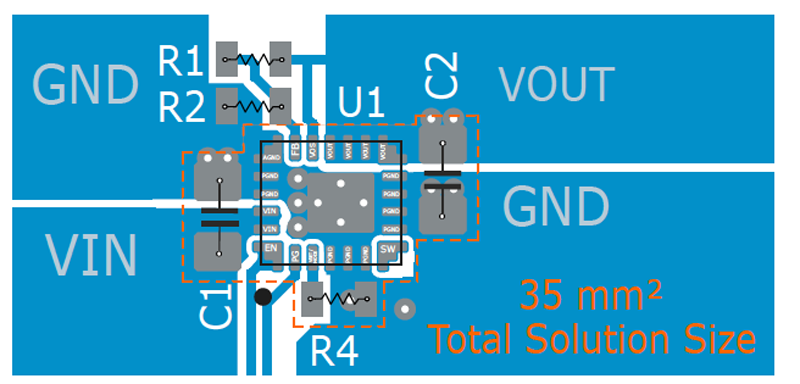
A compact 32 mm2 layout - see Figure 4 - is possible with the TPSM8286xA family, saving valuable PCB space and permitting placement close to the processor's Vin, while achieving high operating efficiency and good thermal performance. Further information on device layout and PCB design best practice can be found in the datasheet. (Mouser link required once product listed)
Click image to enlarge
Figure 4: A suggested layout for an example TPSM8286xA implementation that occupies only 32 mm2 of board space. (source TI)
An evaluation board is also available for the TPSM8286xA family, the TPSM8286xA EVM.
With Intel Enpirion’srecent product EOL announcement that they will no longer accept orders for any Enpirion devices after March 2022, the TI TPSM8282x and TPSM8286xA point of load buck converters are ideal replacement devices.
Placing High Efficiency, Thermally Optimised DC/DC Conversion at Point of Load
Achieving reliable performance from today's highly integrated processors, FPGAs, and ASICs require a detailed approach to architecting power delivery. The use of low profile, compact, and highly efficient DC/DC converters, such as the TPSM8282x, TPSM8282xA and TPSM8286xA, delivers the optimal solution.