IPM, Battery Chemistry, & Charging Algorithms for Wearables
Without silicon, new batteries and new charging algorithms have no way to acquire customers, and without customers – or at least potential customers – they can’t entice ASIC manufacturers to spend development money....
The greatest challenge faced by both new battery chemistry and charging algorithm developers is obtaining an Application-Specific Integrated Circuit (ASIC) design. Without silicon, new batteries and new charging algorithms have no way to acquire customers, and without customers – or at least potential customer - they can’t entice ASIC manufacturers to spend development money to create an ASIC. It’s the classic the chicken or the egg problem. As a result, many battery chemistries and charging algorithms never see the light of day.
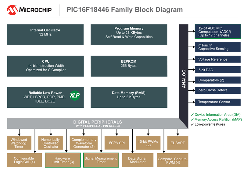
However, the recent introduction of several new microcontroller families with intelligent analog on-chip, such as the PIC16F18446, may represent an alternative to the ASIC battle. These microcontroller families can include a long list of analog and mixed-signal peripherals such as voltage comparators, op amps, Analog-to-Digital Converters (ADCs), Digital-to-Analog Converters (DAC), voltage references, ramp generators, digital Pulse Width Modulations (PWMs), and even logic blocks. Using these blocks, it is then a reasonable leap to build an intelligent charger to show off the new battery or algorithm.
Let’s take an example: A simple charger that first charges constant current, and then switches over to constant voltage (i.e. a standard LiPoly charger profile). Now we have a couple of options, either a DC system, or switched mode. Let’s stick with the DC system for simplicity. So, we need a current source, a voltage source, and a switch to transition from one to the other. Figure 1 shows a classic current source on the left and a voltage source on the right.

Click image to enlarge
Figure 2: Example of a classic current and voltage source
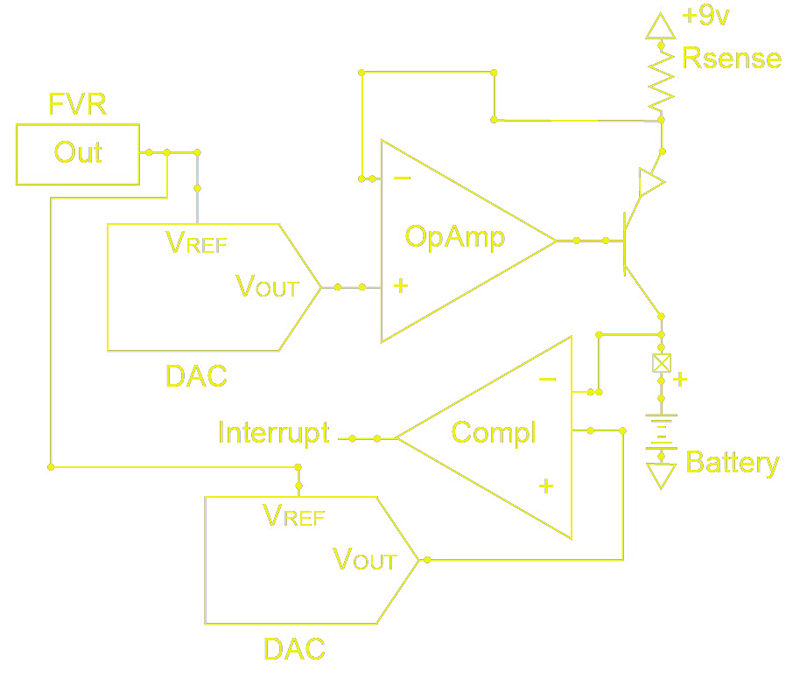
Now if we look closely, we can see that they are pretty much the same. The only difference is the inverting input to the op amp and the value out of the DAC. If we put a comparator on the battery voltage and generate an interrupt when the battery voltage exceeds 4.1V (see Figure 2), then all the firmware needs to do is change the setting for the inverting input on the op amp and load a new value into the DAC.
Click image to enlarge
Figure 3: Example of a battery voltage switch
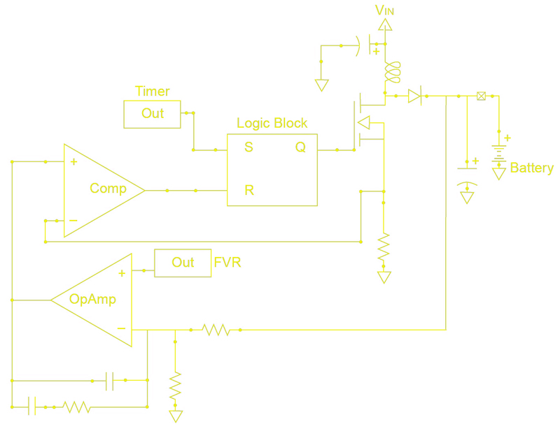
Now, it may not be as simple as this; the charger may be pulsed, or it may require a switch mode charger for efficiency. Well, as far as pulsing the charge voltage/current, the typical op amp peripheral has an enable bit in its control register, so all that is required for pulsing is a periodic interrupt to turn the op amp peripheral on and off. Implementing a switching converter is a little more work, but still doable using on chip peripherals. This is shown in Figure 3.
Click image to enlarge
Figure 4: Example of a switch mode boost converter
The shown circuit is a switch mode voltage source. To make it a switch mode current source, simply change the output feedback from the battery to a current sense resistor between the battery and ground. One thing to note is that the compensation loop will probably also need to change, but even that can be done with two networks and a simple firmware routine to change which input drives the inverting input. Even the switcher can be pulsed in a similar manner to the DC circuit by simply turning off the timer and op amp in the switch.
The end result is that a combination of firmware and peripherals can implement almost any charger function:
1. Constant Current
2. Constant Voltage
3. Pulsed Current
4. Pulsed Voltage
Plus, adding additional features, options, algorithm tweaks, supervisory functions, or even emergency shutdown functions to a design is as simple making a firmware change.
So, using these new microcontrollers, both battery and charger developers can develop proof-of-concept chargers that they can demonstrate for their customers. In fact, for small to medium production runs, the microcontrollers can be preprogrammed, marked with a unique part number and delivered directly to their customer, making the device look and feel just like a custom charger ASIC.
Another point to consider is some customers’ desire to combine multiple power management functions into a single device. These devices can include chargers, backlight drivers, fan controls, and even gas gauge functions, all within a single chip. By generating a microcontroller-based design initially, the battery / charger designer can further boost industry acceptance by licensing their intellectual property either to the customer, or a third party, to design the required composite power device. Customers can then take advantage of preprogramming, and customer part number marking, to further hide their design work from competitors until their design reaches sufficient production numbers to justify the creation of their own composite ASIC design.
Microchip Technology