Author:
Jeff Sorensen, Application Engineer, Helix Semiconductors
Date
01/16/2019
 PDF
PDF
Click image to enlarge
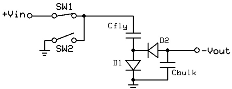
Figure 1: Simple flying capacitor circuit
Charge pump topologies and the precursors to charge pumps have been around for over 100 years. In the drive to make products smaller and more efficient, it may be the time to dust off the old flying capacitor and see what it might be able to do for you.
A “flying capacitor” is simply a capacitor that has both ends switched at the same time, so it is floating (flying), to transfer a charge from one circuit to another. In Figure 1, the positive charge is impressed on the flying capacitor top terminal when SW1 closes connecting Cfly to Vin. Cfly is connected to a series diode (D1 in fig. 1) to ground. SW1 is switched off and SW2 is turned on to now connect the top of Cfly to ground. The bottom end of Cfly, connected to a diode (D2 in fig. 1), is now -Vin and charges the bulk capacitor to hold the now negative charge from the flying capacitor’s bottom side which was previously a forward voltage drop above ground. Do this real fast and you have a cheap negative DC supply for an opamp. The two diodes act as switches so the flying capacitor’s charge has a one-way path during the charge and hold times of the cycle. So, the capacitor’s 0-volt reference point is being changed from its bottom end to its top and this charge is then transferred to the bulk capacitor as a negative voltage, minus the D2 diode’s forward voltage.
Similar low power charge pumps have been used internally in many integrated circuits for their own voltage requirements or as monolithic low-power voltage supplies. A charge pump primarily consists of switches and capacitors and can operate in the kilohertz to megahertz frequency range. The switches can be MOSFETS, diodes, transmission gates, or less commonly these days, bipolar transistors. The capacitors can be any type or size, but when internal to an integrated circuit, they can be quite small and run at very high switching frequencies.
Some of the first products that included charge pump circuits are the RS-232 interface drivers/receivers from Maxim. These 5V parts include charge pump circuits to develop +/- 7V logic levels needed for the RS-232 drivers. Both voltage boost and a negative supply voltage are needed for RS-232 compatibility. Flying capacitor circuits can be configured to do both these functions. They have been used for many years to efficiently generate a needed voltage level without a transformer or complex power supplies when only limited current was required. Charge pumps can be extremely efficient for converting one voltage to another or for generating negative voltages from positive ones as in the MAX232 et al. The Intersil ICL7660 is also a popular negative voltage charge pump that has been second sourced by other IC manufacturers. There are many integrated charge pumps available today that can both boost and generate negative voltages, including some in a single package, such as the MAX865. This device can generate a positive voltage that is twice the input voltage as well as a negative voltage that is twice the boosted voltage. Very few of these types of devices, however, can supply more than 150 mA of current and/or operate at a supply voltage greater than about 12V. An exception that can provide up to 15W and operate at voltages from 12 – 57V is the Helix Semiconductors MxC 200, which will be discussed later.
The current that can be derived from a charge pump depends primarily on three factors; the Rdson (drain-source on resistance) of the switches used, the capacitance value of the capacitors, and the switching frequency. Most, but not all, of the lower voltage integrated charge pumps use CMOS switches with Rdson that can be 150Ω or more. One exception to this is the Linear Tech LTC3216, which is intended to drive a high brightness LED for cell phone cameras or other lighting applications.
Although there are a few different topologies that can be used, the majority use something very similar to Figure 2. The following describes the operation of a typical voltage reducing charge pump. This is essentially the same circuit topology used for the voltage doubler in the MAX865 mentioned earlier but can be used to reduce as well as increase the voltage level.
Click image to enlarge
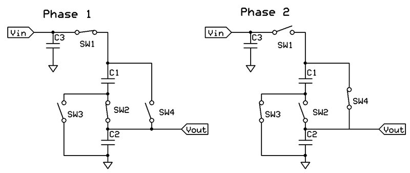
Figure 2. A flexible flying capacitor charge pump circuit
There are two phases for each cycle in this charge pump’s operation for either step down or step up circuit function. In the circuit in figure 2 there are two pairs of switches. For step down operation, in the first phase Sw3 and Sw4 are open and Sw1 and Sw2 are closed to connect the voltage at Vin to the flying capacitor C1 in series with the bulk capacitor C2. Each capacitor is therefore charged to ½ the voltage at Vin. In the second phase, Sw1 andSw2 open and Sw3 and Sw4 close, connecting C1 and C2 in parallel. The net effect of this is that the voltage at Vin is divided in half at Vout. In addition to the voltage now being reduced to half the input level, the current available at Vout is now double the current supplied to the Vin pin. Since there is very little power lost to the switch resistance and capacitor’s ESR, efficiencies of 90-97 percent are usually achieved with sub-1 Ohm low-resistance switches. Even the charge pump devices with higher Rdson can often expect efficiencies of over 80 percent if not loaded too heavily.
If the Vin and Vout ports are reversed, the circuit acts as a voltage doubler. Again using figure 2, when power is applied to the Vout pin with Sw3 and Sw4 closed, both C1 and C2 are charged in parallel. When these switches open and Sw1 and Sw2 are closed, C1 and C2 are placed in series and the voltage at the Vin pin is now twice the voltage applied at the Vout pin. There does also need to be a capacitor, C3, on the Vin pin to store the charge from the series connected capacitors. In this case, the current available at Vin will be half the current supplied to the Vout pin, and the same efficiency or better can be expected when using the charge pump in boost mode.
Charge pumps generally do not regulate the voltages they are used to generate, but some do. For example, the TI TPS60150 flying capacitor charge pump can take voltages from 2.7V to 5.5V and provide a regulated output of 5V. This is a special case and designed to be used where the input voltage supply can vary, such as in a battery powered application. Otherwise if a precise voltage supply is needed, an inexpensive PWM or LDO voltage regulator can be used to regulate the charge pump output.
When using a regulator to generate accurate, stable power for an application, the efficiency is usually also an important concern. By dropping the voltage level to something nearer the voltage needed, a regulator can work more efficiently due to lower switching losses in PWM designs, or lower dissipated power loss a linear regulator. Efficiency is improved when there is a smaller input to output voltage ratio for the regulator to work with. The regulator’s required input headroom, including the charge pump’s droop under load, needs to be factored into the design. It is possible to take advantage of this in a distributed power system. By using charge pumps to drop the voltage level at the source and using small, inexpensive PoL (Point-of-Load) regulators to precisely regulate the voltages at the load, there is less crosstalk and noise distributed through the power rails. Voltage levels can also be made more consistent across the PCB if there is local regulation instead of regulation at a single point. A power plane driven from a charge pump can then be locally regulated to the individual needs of the circuits instead of distributing several different voltages across the board.
All charge pumps using the flying capacitor topology above have one characteristic that needs to be allowed for in the design. When powering up, the output cannot have a heavy load connected to the output. Many charge pumps can deal with some loading, but if all the current is going to the load instead of charging the capacitors, the charge pump may not be able to start up at all. This can be dealt with in several ways. If the output goes to a regulator with an enable pin, the enable pin can be connected to the output of the charge pump, so the charge pump can come up before the regulator is enabled. Some charge pumps have a “Power Good” output that turns on once the output voltage has reached a safe level. In some cases, a switch is used to gate the output on after some time delay has occurred. And in many cases the output load ramps up slowly enough the load does not appear until the charge pump has had time to stabilize.
The MxC 200 is unique in that there are three stages that can be configured to divide or multiply by two, four, or eight, depending on how they are connected. Two of these stages operate 180° out of phase from each other so that when operated in parallel in the divide by four mode, there is very little ripple on the output. When cascaded in a voltage dropping configuration, each stage has twice the current driving capacity of the previous stage, but at half the voltage.
Charge pumps can be connected in parallel to get higher power if needed. Since they don’t regulate, charge pumps don’t have the problem of struggling with each other for control of the output voltage. MOSFET-based charge pumps have a positive temperature coefficient, so they naturally share the load equally rather than one dominating. If one device connected in parallel with other identical charge pumps begins to supply more current, the internal temperature will rise and cause its Rdson to go up, reducing the current for that device. In this way, single or multiple charge pump devices can be used for the raw power distribution and then the power locally regulated to the final voltage where it is needed. Another charge pump alternative for high power is to use a charge pump controller such as the Linear LTC7820 and discrete switches. This product has the gate drivers and control for four MOSFFET switches that uses the same familiar flying capacitor topology that was described earlier. This device is intended for input voltages from 24V to 72V, very high output currents and is a single stage flying capacitor design that can be used for either doubling, halving or generating a negative voltage. In the voltage divider mode, it can supply up to 15A when properly configured with the external MOSFETS. There is also a regulated output version of the part, the LTC2821. The cost for the controller is quite high compared to other complete charge pump devices and still needs the external NMOS switches, so using it in lower power applications is probably not cost effective. For high power, it is well suited and highly efficient, 99 percent according to the manufacturer.
With the availability of charge pump integrated circuits that span nearly the entire power spectrum, maybe the lowly charge pump’s time has come. With the drive to improve efficiency in nearly all electronic product areas, charge pumps have a role in helping reduce waste and making products more attractive to the consumer by reducing the cost of operation and weight (because power supplies can be made lighter and smaller). Looks like the flying capacitor isn’t going away anytime soon.
Helix Semiconductors