Interference immunity on the shop floor
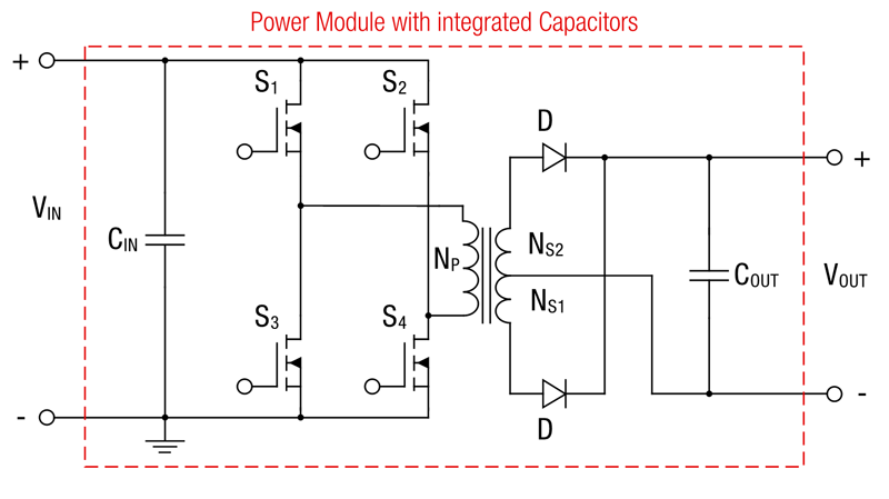
Figure 1: Structure of the isolated MicroModule 1769205132 of the FIMM series. It comprises a semiconductor IC, rectifier diodes, input and output capacitors and a transformer
Industrial environments typically require reliable and interference-free power supplies. Usually, the different components of an industrial plant are powered by DC bus systems. This article explains how such a low-interference bipolar supply in the low-voltage range can be realized.
Typical industrial plants generally require the use of a number of different elements for safe operation, like isolation amplifiers, analog-to-digital converters, isolation of digital circuits, Interfaces/bus isolation as well as measurement and data acquisition. All these applications have in common, that they require the isolation of their supply voltage from the bus voltage.
High efficiency is key
As an isolated DC/DC converter, a power module with galvanic isolation provides a reliable supply for an analog-to-digital converter (ADC) in industrial applications. The isolated MicroModule 1769205132 of the FIMM series (Fixed Isolated MicroModule), uses chiplet SIP technology to reduce the dimensions by 80%, resulting in a module with the dimensions 9x7x3.1 3mm3. The board space requirements are reduced by more than 50% compared to a standard SMT-8 power module (9x7 mm2 versus 13.2x12.2 mm2).
The MagI³C power module 1769205132 is based on a full bridge topology. The module integrates a switching power stage, control circuitry, rectifier diodes, input and output capacitors and a transformer (Figure 1). Since there is no feedback path from the output to the input, the duty cycle is fixed at 50 % and is independent of the load. The output voltage is unregulated and is determined by the transformer turns ratio. The output power of 1 W can be provided up to an ambient temperature of TA=100°C without any output current derating. The parasitic coupling capacitance between the primary and secondary side has a typical value of 8 pF due to the design, which ensures a high degree of decoupling from high-frequency interference and mitigates the potential for common-mode interference to propagate from the primary switching side to the secondary side of the converter. With an efficiency of 91 % it is the "best-in-class" in the complete isolated power module portfolio of Würth Elektronik.
Powering sensitive ADCs and sensors
Applications such as measurement and data acquisition are often built with ADCs, which convert the analog measured values, such as a temperature value or a current, into a digital quantity. For the acquisition of positive and negative measurement signals, a dual voltage supply is required. Usually a supply of ±5 V is used in such applications.
The resolution that an ADC can provide, i.e. how many bits it effectively makes available, depends, among other things, on the noise component of the supply voltage.
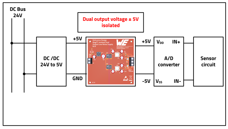
The red circuit board in the application in Figure 2 generates a galvanically isolated dual voltage of ±5 V from an input voltage of 5 V. Special features of the circuit are a very low residual ripple at the output and a broadband decoupling between input and output.
Click image to enlarge
Figure 2: Example of a sensor application using a decoupled dual voltage supply (red board)
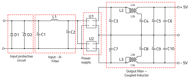
The dual voltage supply consists basically of four different functional blocks (Figure 3):
Clcik image to enlarge
Figure 3: The decoupled dual-voltage supply (red board in Figure 2) includes a protection circuit on the input side, a filter on the input side, a power module (FIMM) and a filter on the output side
1) Input protection circuit: the protection circuit integrates reverse polarity protection and voltage transient protection.
2) Input filter: The first filter stage serves to attenuate conducted interference levels. Harmonics generated by the switching operations of the DC/DC converter, in the direction of the supplying source, are reduced in their amplitude. On the other hand, interference can reach the power module via the power supply and is attenuated by the filter.
3) Power module: The power module itself converts the voltage and provides galvanic isolation between the input and output.
4) Output filter: The current supplied by the power module is a superposition of a DC current with an AC component. The AC component is the part that is reduced in amplitude by the filter in order to provide a "clean" DC voltage for the application to be supplied, such as an ADC.
Input protection circuit
The protective circuit on the input side has a two-stage design (Figure 3 left).
The diode D1 fulfills two tasks. It protects the input from negative transient interference and prevents damage to the input of the power module in case of reverse voltage polarity. With a forward voltage of 0.3 V @ 0.3 A, it clamps the voltage to a value below the maximum operating value specified for the power module.
Diode D2 protects the circuit from positive voltage transients. At a positive voltage transient between 6 to 9 V from the cathode to the anode, diode D2 conducts. The effective clamping voltage is then typically 5.7 V and thus in the range of the absolute maximum rating of the power module.
Input filter
The power module operates with a typical internal switching frequency of 300 kHz. The upstream power supplies typically have a switching frequency of 50 to 500 kHz. This results in a filter combination that already has an attenuation of approximately 50 to 75 dB at approximately 100 kHz in order to filter the transient interferences.
The combination of C1, L1 and C2 forms a π-filter structure. The values of the individual filter components were chosen with the aim of providing an insertion loss of approximately 50 dB starting at 100 kHz.
Figures 4 shows the curve of the insertion loss of the first filter stage. Here it can be clearly seen that from 50 kHz an attenuation of approximately 80 dB is achievable.

Click image to enlarge
Figure 4: Plot of the insertion loss of the first filter stage as a simulation in RedExpert. One can clearly see here that already from 50 kHz an attenuation of approx. 80 dB is achieved
The calculation/simulation can be carried out with the filter designer in REDEXPERT [1]. The tool uses the real properties of the components based on measurements for the calculation. This way, the simulated results correspond better with the real components. The calculation of the insertion loss was carried out with a source and load impedance of 50 Ω. Essential for a high insertion loss in practice is an RF-compatible design that avoids coupling between the components.
Output filter
Due to its principle of operation, the output voltage of a DC/DC converter does not provide a pure DC voltage as, for example, with a linear regulator. It is rather a combination of a DC voltage with a superimposed AC component. The AC component is specified in the data sheet as an "output voltage ripple & noise" value in mVPP, indicating the peak-to-peak amplitude of the output voltage. ADC circuits are sensitive here, as they can only work optimally with a small interference signal from their supply, which must be lower than the resolution of the ADC.
The circuit shown in Fig. 3 on the right is a filter that reduces the interference voltage of the FIMM on the output side. The linear two-port filter consists of a coupled inductance, with windings L2a/L2b and capacitors C3 and C4.
Winding L2a conducts the DC component to the load (like a "smoothing choke"), while the AC component flows to ground via winding L2b and capacitor C4. The impedance behavior of capacitor C4 causes it to discharge the high-frequency component to ground.
The magnetic coupling between the two windings, i.e. the negative feedback inductance, which is described by the coupling factor k, is essential for the filter function.
Due to the winding orientation of the two windings of the coupled inductance, the AC portion of the current flowing through winding L2b is transferred to winding L2a. The AC portion of the current is then superimposed on the DC (AC) current, whereby the AC portion is cancelled out in the load current as well as compensated via the magnetic coupling and thus reduced.
The factor k is used to indicate the coupling between two coil windings, with a value of 1 indicating 100% coupling between the two windings. Ideally, a k of less than 0.98 should be used. The coupled inductor WE-DD 744877220 used here has a coupling factor of approximately 0.98. The capacitors used must have the lowest possible ESR value in order to achieve the desired filter effect. For example, the aluminum polymer capacitor WCAP-PTHR 870055673002, which has an ESR value of less than 100 mΩin the frequency range from 1 kHz to 50 MHz, can be used here as a 22-µF capacitor.
FIMM layout recommendation
Care has to be taken that the FIMM module has two separate ground connections: pins 1 and 2 for the primary side and pins 3 and 4 for the secondary side.
More detailed information on the layout can be found in the data sheet of the FIMM [2] in the section "DESIGN EXAMPLE". A layout recommendation for ALTIUM is available from the online catalogue [2] in the "DOWNLOADS" section.
References
[1] RedExpert Filter-Designer: https://redexpert.we-online.com/we-redexpert/en/-/emifd-embedded/
[2] Data sheet of the FIMM In the section "DESIGN EXAMPLE": https://www.we-online.com/katalog/en/MAGIC-FIMM


.jpeg)