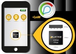
Lattice Semiconductor announced their latest ultra-low-density iCE40™ FPGAs, delivering the world’s most flexible, single-chip sensor solutions for making a new generation of context-aware, ultra-low power mobile devices possible. The new additions to the iCE40 FPGA family allow customers to integrate more functions into a smaller space. In packages as small as 1.4mm x 1.48mm x 0.45mm, they are small enough and affordable enough to fit almost anywhere, reducing board space and system complexity.
With hard IP for strobe generators, I2C and SPI interfaces, the new iCE40LM FPGAs deliver near-zero latency to the mobile market, enabling context-aware systems with the real-time capturing of user and environmental inputs with minimal delay or error. This gives designers a platform for their mobile products to deliver media-rich experiences based on movement, travel direction, location and other interactions with the environment.
The small size of the new iCE40 FPGAs enables integration of advanced functions such as IrDA, barcode emulation, service LED, and more in a single chip with available logic for addition customer defined functions. Moreover, Lattice has demonstrated the iCE40LM FPGA solution can reduce power consumption by100x over traditional application processor-only implementations, thus increasing battery life to bring more value to the end user.
“The combination of ultra-low active power and the world’s smallest sensor management solution enables a completely new class of intelligent devices that know where they are and what they are doing,” said Joy Wrigley, senior product line manager for Lattice’s Ultra-Low Density Families. “We’re investing in packaging technologies that integrate more function and shrink system size, allowing OEMs to affordably integrate a greater variety and number of sensors into their mobile systems. Context awareness is truly a game changer in the mobile industry and iCE40LM sensor solutions enable designers to access this differentiation immediately.”
The new iCE40LM FPGAs give mobile device system architects the ability to add and/or customize sensor management functions and capabilities using a single, simple platform that can be implemented across different designs. The new additions include the iCE40LM 4K, iCE40LM 2K, iCE40LM 1K FPGAs and consume very little power, just under 1 mW in active mode.
Meanwhile, the iCE40LP FPGA product line is being expanded through the addition of a new 16-ball WLCSP (wafer-level chip-scale) package for both the iCE40LP 640 FPGA and iCE40LP 1K FPGA to further drive down the footprint of the iCE40 family. Critical for ‘the internet of things’ and ‘always-on’ applications, the new additions to the iCE40 family are tiny, measuring just 1.4mm x 1.48mm x 0.45 on an advanced 0.35mm ball pitch packaging.
 PDF
PDF