Transforms board power & digital management
At the company's press launch in Munich, Germany, Gordon Hands, Director of Strategic Marketing for Lattice's Low Density and Mixed Signal Solutions, presented Lattice's next-generation programmable device technologies. Gordon was also instrumental in the definition and launch of the Lattice ECP/ECP2/ECP2M FPGA families, the Lattice XP/XP2 non-volatile FPGAs, the MachXO family of programmable logic devices and the ultra low power 4000ZE CPLD family. Lattice Semiconductor Corporation has announced its third-generation mixed-signal devices, the Platform Manager™ family. The programmable Platform Manager devices are expected to simplify board management design significantly by integrating programmable analog and logic to support many common functions, such as power management, digital housekeeping and glue logic. By integrating these support functions, Platform Manager devices not only reduce the cost of these functions compared to traditional approaches, but also can improve system reliability and provide a high degree of design flexibility that minimizes the risk of circuit board re-spins.

"Lattice first transformed board power management design with its Power Manager II products, which have been enthusiastically adopted across a wide variety of systems due to the improvements in cost, reliability and design cycle time they enable," said Gordon Hands, Director of Marketing for Low Density and Mixed Signal Solutions. "We expect that customers will rapidly adopt the new Platform Manager products, as they expand these same benefits across a broader range of functions."
Platform Manager devices are expected to be used in a broad range of applications where the complexity of the board management functions can benefit from the integrated capabilities that they provide. Typical applications are expected to include wireless infrastructure, networking core equipment, server, data storage and high-end industrial instrumentation.
Platform Manager devices are expected to be used in a broad range of applications where the complexity of the board management functions can benefit from the integrated capabilities that they provide. Typical applications are expected to include wireless infrastructure, networking core equipment, server, data storage and high-end industrial instrumentation.
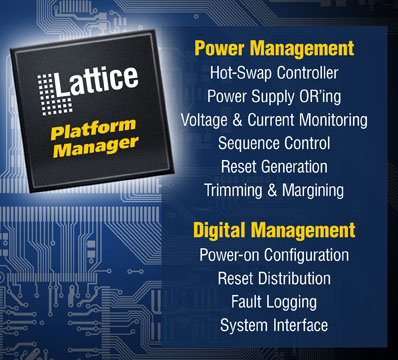
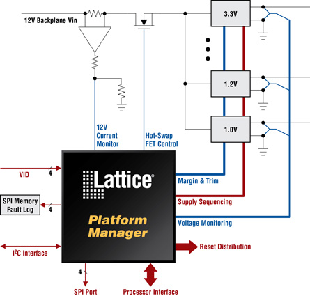
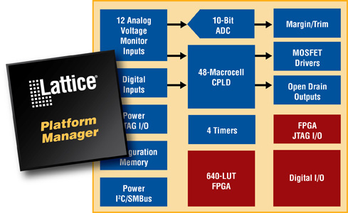
Description The Lattice Platform Manager integrates board power management (hot-swap, sequencing, monitoring, reset generation, trimming and margining) and digital board management functions (reset tree, non-volatile error logging, glue logic, board digital signal monitoring and control, system bus interface, etc.) into a single chip. The Platform Manager device provides 12 independent analog input channels to monitor up to 12 power supply test points. Up to 12 of these input channels can be monitored through differential inputs to support remote ground sensing. Each of the analog input channels is monitored through two independently programmable comparators to support both high/low and in-bounds/ out-of-bounds (window-compare) monitor functions. Up to six general purpose 5V tolerant digital inputs are also provided for miscellaneous control functions. There are 16 open-drain digital outputs that can be used for controlling DC-DC converters, low-drop-out regulators (LDOs) and opto-couplers, as well as for supervisory and general purpose logic interface functions. Four of these outputs (HVOUT1-HVOUT4) may be configured as high-voltage MOSFET drivers. In high voltage mode these outputs can provide up to 12V for driving the gates of n-channel MOSFETs so that they can be used as high-side power switches controlling the supplies with a programmable ramp rate for both ramp up and ramp down. The board power management function can be implemented using the on-chip 48-macrocell CPLD. The status of all of the comparators on the analog input channels as well as the general purpose digital inputs are used as inputs by the CPLD array and all digital outputs (open-drain as well as HVOUT) may be controlled by the CPLD. Four independently programmable timers can create delays and time-outs ranging from 32μs to 2 seconds. The Platform Manager device incorporates up to eight DACs for generating trimming voltage to control the output voltage of a DC-DC converter. Additionally, each power supply output voltage can be maintained typically within 0.5% tolerance across various load conditions using the Digital Closed Loop Control mode. The on-chip 10-bit A/D converter can both be used to monitor the VMON voltage through the I2C bus as well as for implementing digital closed loop mode for maintaining the output voltage of all power supplies controlled by the monitoring and trimming section of the Platform Manager device. The FPGA section of the Platform Manager is optimized to meet the requirements of board management functions including reset distribution, boundary scan management, fault logging, FPGA load control, and system bus interface. The FPGA section uses look-up tables (LUTs) and distributed memories for flexible and efficient logic implementation. This instant-on capability enables the Platform Manager devices to integrate control functions that are required as soon as power is applied to the board. Power management functions can be integrated into the CPLD and digital board management functions can be integrated into the FPGA using the LogiBuilder tool provided by PAC-Designer® software. In addition, the FPGA designs can also be implemented in VHDL or Verilog HDL through the ispLEVER® software design tool. The Platform Manager IC supports a hardware I2C/SMBus slave interface that can be used to measure voltages through the Analog to Digital Converter or is used for trimming and margining using a microcontroller. There are two JTAG ports integrated into the Platform Manager device: Power JTAG and FPGA JTAG. The Power JTAG interface is used to program the power section of the Platform Manager and the FPGA JTAG is used to con-figure the FPGA portion of the device. The FPGA configuration memory can be changed in-system without interrupting the operation of the board management section. However, the Power Management section of the platform Manager cannot be changed without interrupting the power management operation. About the Platform Manager family The Platform Manager product family consists of two devices, the LPTM10-1247 and LPTM10-12107. The LPTM10-1247 device can monitor 12 voltage rails and supports 47 digital I/O, while the LPTM10-12107 monitors up to 12 voltage rails and supports 107 digital I/O. Functionally, these devices include both a power management section and a digital board management section. The power management section consists of a programmable threshold, precision differential input comparator block with an accuracy of 0.7%, a 48-macrocell CPLD, programmable hardware timers, a 10-bit analog to digital converter and a trim block for the trimming and margining of supplies. The digital board management section consists of a 640-LUT FPGA and programmable logic interface I/O.
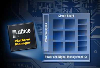
Transforming board management design with platform manager devices Modern circuit boards use devices such as CPUs, FPGAs and ASICs to perform the primary processing functions. These primary function devices require multiple board-mounted power supplies that need to be turned on and off in a specific sequence, monitored for faults and trimmed for voltage accuracy. In addition, the input power to the board often requires redundant power management and, in the case of plug-in boards, hot-swap functionality. All the functions that control various power rails are collectively called power management. After all supplies are turned on, the system requires digital support functions such as reset distribution, start-up configuration control for FPGAs and ASSPs, watchdog timers and a system bus interface for a microcontroller. These digital support functions are collectively called digital management. Power and digital management together are often referred to as board or platform management. Lattice's new Platform Manager family provides a single-chip solution that integrates all of these power and digital management functions.
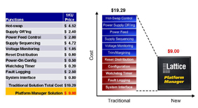
The programmable Platform Manager device, with its ability to integrate both power management and digital management functions, reduces the number of board components, saving time and board area, and reducing design risk. The traditional methods of designing with a collection of unique single-function ICs for power management, and complex design partitioning across multiple programmable devices for digital support functions, are simply replaced by the single chip Platform Manager device. It is anticipated that in many cases the Platform Manager can cut the bill-of-material cost by 50%. When implemented correctly, board power management can dramatically improve system reliability, because when operation under abnormal or faulty conditions is prevented, damage to components and corruption of system memory is avoided. With the traditional approach to power management, designers often reduce the number of supplies monitored, the speed of response to errors and the accuracy of monitoring in order to meet cost targets, compromising board reliability. The Platform Manager avoids this compromise with its low cost and ability to monitor up to 12 rails with 0.7% accuracy and a <65uS response to power supply faults. In addition, the Platform Manager device provides several benefits compared to traditional design methodology, such as increased flexibility, on-board reprogrammability and software-based design and simulation. In those cases where these benefits help to avoid a board re-spin, weeks or even months can be saved from the project schedule. Design Software Support The Platform Manager product family will be supported by PAC-Designer® 6.0 and the Starter version of ispLEVER® 8.1 SP1 design software tools. There is no charge for either software package. For information about how obtain a copy, go to www.latticesemi.com/ptm
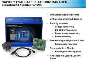
To accelerate design time using the Platform Manager, Lattice will provide four free reference designs and three free IP cores that implement common functions such as Fault Logging into Non-volatile Memory, Closed Loop Margining and Interface to I2C or SPI bus masters. Detailed information about the reference designs and IP cores may be downloaded from the Lattice website at www.latticesemi.com/ip. In addition, a Platform Manager design development kit, containing an evaluation board complete with demonstration code and documentation, can be purchased for $109. This board allows users to see known good hardware in five minutes and to recompile the provided source code to get to a known good starting point in thirty minutes. For more details and buying information please visit: www.latticesemi.com/ptmdevkit A video demonstration of the Platform Manager can be viewed here: www.latticesemi.com/ptmEN Pricing and availability The new Platform Manager devices are available in commercial and industrial temperature ranges, and are available in environmentally friendly Lead-Free/Halogen-Free packages. High volume pricing for the LPTM10-1247 device in a 128-pin TQFP package is $3.75. Samples are available now. www.latticesemi.com


