Energy efficiency also reduces electronic waste
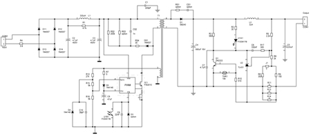
In 2009 the EU decided to abandon incandescent lighting step by step, starting with the poorest efficiency bulbs in 2010. Higher efficiency alternatives like CFL lamps or high efficiency LEDs are readily available but attention must be paid to the actual design to confirm that it is as environmentally friendly as possible. Environmentally friendly does not just refer to the components themselves but the number of components used and their lifetime - things that are meant by the term ecodesign. Longer lifetime of electronic equipment, resulting in less waste, is achieved by reducing the number of components and increasing their durability. This article explores the design of a primary side regulated (PSR) off-line ballast for LED with constant current output. The low component count and long lifetime makes the design both cost-effective and environmental friendly. The majority of electronic ballasts for high power LEDs operate in constant current mode. Due to the V-I characteristic of a LED a current limiting element is mandatory for stable operation. Consequently, the most popular approach is to put a number of LED in series and drive them with a current source. The traditional approach of implementing a constant output current power supply is to measure the load current, e.g., with a shunt resistor and feed this signal back to the PWM controller. Actually, unless one doesn't care about power dissipation and efficiency, the signal generated by the shunt is too small and has to be amplified in some way. This can be done by a simple single stage BJT amplifier or an integrated operational amplifier. The BJT has an advantage of having a built-in �reference voltage', the forward voltage VBE of the base-emitter diode. But the latter is not very accurate and has a considerable negative temperature coefficient. If the BJT amplifier is used in cost-effective applications like mobile phone chargers, consequently there is some kind of compensation for this temperature coefficient of VBE as e.g. the PTC THR1 in the schematic Figure 1. The schematic further shows that there are additional things to consider when designing a current source PSU. At no load current the output voltage would rise to an unacceptable high value. Hence there is an additional voltage regulation loop that is implemented with the reference/error amplifier KA431. Finally, if the output has to be isolated from the mains input, an optocoupler is needed in the feedback path. This optocoupler is an often overlooked component that can limit the lifetime of a PSU.
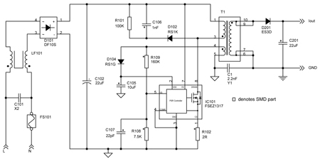
While in consumer applications a lifetime of say 10000h is excellent and most applications don't need such a long one, the situation in lighting applications is different. Doubtless one expects the ballast to live at least as long as the light source itself. But since in a lot of applications electric lighting may be used a significant part of the day, one doesn't want to replace the electronics each time the light source is defective but expects a lifetime of up to 50000h from the ballast. Actually, electrolytic capacitors are the electronic components with the shortest lifetime and in fluorescent lamp ballasts, one with extraordinary long lifetimes and hence, high cost are used. Both the electrolytic capacitors' and the optocouplers' lifetimes are reduced by high temperatures. Unlike fluorescent lamps LEDs must be cooled and often the complete luminary is used as a heatsink. As a result the ambient temperature of the ballast and in turn, that of the optocoupler will be quite high. Thus, it would be advantageous to design LED ballasts without optocouplers. For constant voltage output there is a well-known solution: the primary side regulated flyback. A primary side regulated PSU works without any direct feedback path from the secondary, reducing part count and cost while increasing reliability considerably. This topology has recently been extended to constant current output. The actual ballast is designed around the FAN103, a dedicated PSR Flyback controller with patented constant current regulation circuit. The schematic of the ballast is shown in Figure 2 and looks quite unspectacular at first glance. Nevertheless the ballast can deliver up to 22V, enough to drive up to five LEDs in series, at a current level of up to 700mA from a universal mains input. The output current can be selected to be 350mA or 700mA by jumper J101 that changes the value of the current sense resistor. If a bigger transformer is used (EF25 core instead of EF20) and the current sense resistors R102 and R103 are adjusted, even 1A output is easily possible.
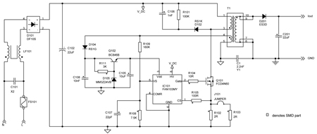
A detailed description of the operation of the ballast, that is available as a completely assembled evaluation board, is given in the following section. C101 and LF101 together with C1 form an EMI filter followed by the rectifier bridge D101 and the filtering capacitor C101. Initially C105 is charged via the internal start-up circuit of the controller to the device's start voltage. When the latter is reached, oscillation begins and the MOSFET is controlled by a PWM gate signal. The topology of the PSU is that of a flyback. When the MOSFET is in the off state, D201 at the secondary of the transformer is conducting and the energy stored in TR101 is transferred to C201 and the load. R101, C106 and D102 form the well-known clamping network the limits the voltage spikes due to the energy stored in the leakage inductance of the transformer. In steady state, the controller is supplied from a separate winding of the transformer. The voltage of this winding is rectified by D104 and filtered by C108. A simple linear regulator consisting of R111, D105 and Q102 limits the voltage at the VDD pin of the controller to 24V maximum. This is necessary since the ballast is designed to operate even with a single LED connected to the output i.e., voltages down to 2.8V in the worst case. The voltage across the supply winding of the transformer will vary with the same ratio of 17V/2.8V = 6.07. Since the minimum operating voltage of the FAN103 may be 7.25V the maximum VDD would be 44V, which would destroy the device.
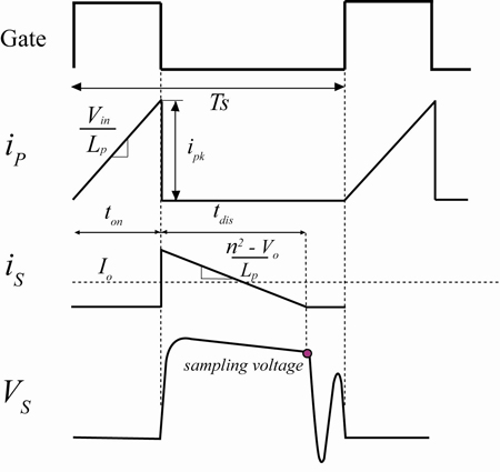
The voltage of the supply winding is used to do the regulation of both, output current and voltage. In case of high load resistance the PSU is not in constant current but constant voltage mode. The FAN103 uses quite an elaborate method of regulating the output voltage tightly. The voltage of the supply winding, that has almost the same waveform but lower voltage level as the drain of the MOSFET, is scaled by the divider R109 and R108, noise filtered with C107 and feed to the VS pin. Internally the voltage is sampled and the zero crossing of the current through D201 is determined by monitoring the rate of change of VS since the sample at this point gives the best estimate and hence regulation of the output voltage. As load current increases, the output goes from constant voltage into constant current mode. To understand how the latter mode works a bit of math is indispensable. In DCM the output current IO of a flyback is (see Figure 3)
 Using the transformer winding ratio
  the formula for the output current can be written with peak primary side current:
 Finally, the peak primary current is given by
  and the concluding equation is
 Obviously the first factor is constant for a given design, VCS is the measured voltage at the CS pin and tdis is determined in the same step the zero crossing of ID201 is determined. In order to achieve a constant output current, the feedback loop has to regulate the on time of the MOSFET such that the product
  is kept constant.
From the equation above it's clear that the output current for a given design is inversely proportional to the sense resistor RCS i.e., double the value gives half the output current.
Having a closer look at the schematic one will recognize that there is only a single electrolytic capacitor: C102. For universal input and the given power level of about 15W a capacitance value around the used 22uF is necessary. But if the input is limited to European power line voltage the latter can be made as small as 6.8uF, a value that is readily available as film capacitor. As mentioned earlier, replacing the electrolytic capacitor results in a ballast with an extraordinarily long lifetime, possibly longer than that of the LED itself.
The component count can be reduced even further by using the FSEZ1317, a Fairchild Power Switch (FPS™), incorporating the controller and a 600V / 1A MOSFET in one package. With this device the output is limited to 350mA. If the output is designed now to drive a minimum of three LED instead of one, the simple linear regulator around Q102 can be omitted as well. The resulting schematic in Figure 4 contains only 19 components in total but nevertheless implements a complete isolated constant current driver for high power LED. It goes without saying, that the reliability of the ballast will be increased at the same time.
is kept constant.
From the equation above it's clear that the output current for a given design is inversely proportional to the sense resistor RCS i.e., double the value gives half the output current.
Having a closer look at the schematic one will recognize that there is only a single electrolytic capacitor: C102. For universal input and the given power level of about 15W a capacitance value around the used 22uF is necessary. But if the input is limited to European power line voltage the latter can be made as small as 6.8uF, a value that is readily available as film capacitor. As mentioned earlier, replacing the electrolytic capacitor results in a ballast with an extraordinarily long lifetime, possibly longer than that of the LED itself.
The component count can be reduced even further by using the FSEZ1317, a Fairchild Power Switch (FPS™), incorporating the controller and a 600V / 1A MOSFET in one package. With this device the output is limited to 350mA. If the output is designed now to drive a minimum of three LED instead of one, the simple linear regulator around Q102 can be omitted as well. The resulting schematic in Figure 4 contains only 19 components in total but nevertheless implements a complete isolated constant current driver for high power LED. It goes without saying, that the reliability of the ballast will be increased at the same time.
Today's designers of electronic devices toned to keep the environmental impact of their designs in view. This does not only concern energy efficiency of the application but reducing electronic waste as well. By developing products with long lifetime and low component count that offer high efficiency, designers can come a step closer to this objective. www.fairchildsemi.com