Leti's local-strain techniques in FD-SOI fabrication to improve next-gen performance & energy use
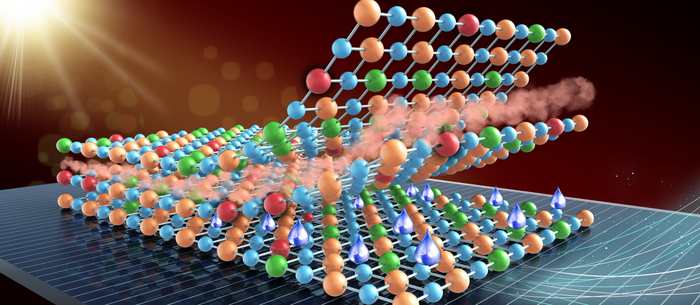
CEA-Leti announced it has developed two techniques to induce local strain in FD-SOI processes for next-generation FD-SOI circuits that will produce more speed at the same, or lower, power consumption, and improve performance. The local-strain solutions are dual-strained technologies: compressive SiGe for PFETs and tensile Si for NFETs. In addition to clearing the path to improved performance in FD-SOI technology, they preserve its excellent electrostatic integrity and its in situ performance tunability, due to back biasing.
The two techniques Leti developed can induce local stress as high as 1.6 GPa in the MOSFETs channel.
The first relies on strain transfer from a relaxed SiGe layer on top of SOI film. In a recent paper in the ECS Journal of Solid State Science and Technology, Leti researcher Sylvain Maitrejean described how with this technique he was able to boost the short-channel electron mobility by more than 20 percent compared to unstrained reference. This shows significant promise for enhancing the on-state currents of CMOS transistors and thus for improving the circuit’s speed.
The second technique is closer to strain memorization methods and relies on the ability of the BOX to creep under high-temperature annealing. At SSDM 2015 in Japan, Leti researchers showed that with this local-stress technique they can turn regular unstrained SOI structures into tensile strained Si (sSOI), for NFET areas. Moreover, this “BOX-creep” process also can also be applied to compressive strain creation, as presented at the 2015 Silicon Nanoelectronics Workshop (SNW) conference.
Strained channels enable an increase in the on-state current of CMOS transistors. As a result, the corresponding IC circuits can deliver more speed at the same power, or reduced consumed power and longer battery life at the same performance.
They also have been proven to be an effective way to increase performance of n and p MOSFET transistors via mobility enhancement of electrons and holes. These kinds of techniques enable boosting of the carrier transport in the CMOS channels, and thus increasing the on-state currents. Beginning with the 90nm node, this strain option has been one of the main approaches of the microelectronics industry for improving the IC speed in bulk transistors. While it was not necessary at the 28nm node for FD-SOI, it becomes mandatory beyond the 22/20nm node.
“Leti has continuously focused on improving and fine-tuning FD-SOI technology’s inherent advantages, since pioneering the technology 20 years ago,” said Maud Vinet, head of Leti’s Advanced CMOS Laboratory. “These two new techniques broaden the capabilities of Leti’s FD-SOI platform for next-generation devices, and further position the technology to be a vital part of the Internet of Things and electronics products of the future.”
CEA Tech-Leti